With the rapid development of information technology, based on the advantages of ARM in embedded systems and the wide application of CAN bus, more and more ARM processors have their own CAN controllers inside, which greatly facilitates developers to CAN. Development of the bus. This topic is based on ARM2104 microprocessor CAN bus system node development, using CAN bus can install the node controller directly in the field, the data is processed and sent to the bus, which realizes the all-digital transmission of information and improves the transmission. Anti-interference ability increases the amount of information transmitted.
Overall design
The CAN bus system node is designed in this subject, and the system node structure is shown in Figure 1.

Figure 1 System node structure
CAN bus system application requirements: CAN bus interface expansion, point-to-point communication.
The design of the CAN node is mainly the design of the circuit between the CAN communication controller and the microprocessor, between the CAN bus transceiver and the physical bus. The microcontroller is mainly responsible for the initialization of the CAN controller, the data transmission with the CAN controller, and processing according to the predetermined program; the CAN communication protocol is mainly completed by the CAN controller, and the CAN controller is mainly responsible for the data to the CAN message. The form is passed, and the system is diagnosed, tested, and processed on the CAN bus. The CAN bus transceiver is the interface between the CAN controller and the CAN bus. The physical level is converted. The function is to increase the communication distance. Improve the system's instantaneous anti-interference ability, protect the bus, and reduce radio frequency interference (RFI).
Usually a complete CAN node should consist of three parts: a microcontroller, a CAN controller, and a CAN transceiver. Currently widely used CAN bus devices have two major categories: one is an independent CAN controller, and the other is a microcontroller with on-chip CAN.
CAN node hardware circuit design
The design of each interface circuit for the CAN node hardware circuit is: CAN interface circuit, CPU module, peripheral circuit (reset circuit and JATG interface circuit). The CPU and power supply circuit are shown in Figure 2 below:
Figure 2 CPU and power module
The LPC2104 uses two sets of power supplies, and the I/O power supply is a 3.3V application system. First, the power supply DW1 rectifies the power supply, filters it through C1 and C3, then regulates the power supply to 5V through the 78M05, and then uses the LDO chip (low differential voltage power supply chip) to regulate the output of 3.3V and 1.8V. The LD0 chip adopts S-1131B33UC and S-1131B18UC, which are characterized by large output current, high precision, high stability and low power consumption.
The matching diagram of the CPU chip and controller SJA1000 in the design is shown in Figure 3.
Figure 3 analog bus hardware diagram
Software design of CAN node
The software design of the CAN node mainly includes the programming of the ARM processor and the design of the SJA1000 driver. After the hardware circuit is determined, the main functions of the system control will depend on the software. Whether the system can work normally and reliably, in addition to the reasonable design of the hardware, is inseparable from the software design with perfect functions.
The software program flow chart is shown in Figure 4 below:
Figure 4 main program flow chart
The GPIO used by the configuration package must be in the file config.h. The program listing is shown in Listing 1. The program list (1) sets the width of the address bus and can only be one of the three values ​​of 8, 16, and 24. . Listing (2) sets the signal AD0 to correspond to GPIO, where 0 corresponds to P0.0, 1 corresponds to P0.1, and so on. The other signals of the address/data bus are sequentially defined based on this signal. The list (3) signal ALE corresponds to GPIO, where 0 corresponds to P0.0, 1 corresponds to P0.1, and so on. The list (4) signal WR corresponds to GPIO, where 0 corresponds to P0.0, 1 corresponds to P0.1, and so on.
List of Program Lists 1 Configuring GPIO for Bus Usage
#define ADDR_N_BIT 16 (1)
#define AD0_PIN_NUM 8 (2)
#define ALE_PIN_NUM 0 (3)
#define WR_PIN_NUM 1 (4)
#define RD_PIN_NUM 4 (5)
#include"exbus.h" (6)
The CAN controller of this system adopts SJA1000. Before the microcontroller communicates normally, it must first load in the corresponding address register to determine the receiving identification code, bus receiving baud rate and output control. This is the CAN controller. initialization. The CAN bus controller SJA1000 used in the system is compatible with both CAN2.0A and CAN2.0B versions. The system design is designed with the CAN2.0A BasIC CAN as the protocol standard.
Before testing the program written before, first determine the chip select address of SJA1000 and make sure there is no conflict with other external memory. Secondly, the microprocessor's control access to the SJA1000 is to access the internal registers of the SJA1000 in the form of an external memory. Therefore, the access address of the SJA1000 internal register when the microprocessor accesses the SJA1000 should be correctly defined.
After testing the entire process, the SJA1000 has eight different interrupts that allow the host controller to immediately act on certain states of the CAN controller. Once the CAN generates an interrupt, the SJA1000 sets the interrupt output (pin 16) low until the host controller takes action on the interrupt by reading the SJA1000 interrupt register, interrupts after the main controller responds, or receives the INFO. For more valid data, the SJA1000 immediately sets the interrupt output to low again. The data is received by interrupt reception. P0.16 of LPC2104 is set to external interrupt INT. The whole data receiving module is composed of data receiving function void ReceivEDAta(uint8 *Rt) and interrupt processing function CANException(void). When the SJA1000 receives the CAN bus data, the LPC2104 generates an external interrupt INT by receiving the interrupt to enter the interrupt processing function, and then processes the received data.
It can be imagined that in the whole process of software design of the CAN node, after the hardware circuit is determined, the main functions of the system control will be realized by software, and can work normally and reliably.
in conclusion
With the ARM chip as the main controller, the CAN bus as an embedded system for data transmission is widely used. At the same time, the reliability of CAN communication has become one of the key parts that affect system performance.
Taking LPC2104 as an example, this paper gives a more general hardware connection method between a kind of microprocessor and CAN controller SJA1000. The reliability design of CAN bus node is carried out. The CAN controller can be used to install the node controller directly. At the scene, the data is processed and sent to the bus, which realizes the all-digital transmission of information, improves the anti-interference ability of the transmission, and increases the transmission amount of information.
The design is now available in the body control system in the factory floor and is reliable.
Instruction Manual
1. Features
Clock display, 10 sets of adjustable timed power control, randomized power control, manual switch and optional DST setup.
2. First time charging
This timer contains a rechargeable battery. It is normal that the new/old model runs out of battery if it wasn`t being charged for a long period of time. In this case, the screen will not turn on.
To charge : simply plug the timer to a power outlet. The charging time should take at least 15 minutes.
If the screen doesn`t light up or displays garbled characters, simply reboot the system by pressing the [RESET" button.
3. Set clock
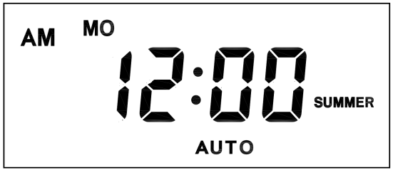
Hold [CLOCK" button and [WEEK" button to adjust week.
Hold [CLOCK" button and [HOUR" button to adjust hour.
Hold [CLOCK" button and [MINUTE" button to adjust minute.
Hold [CLOCK" button and [TIMER" button to select 12 hour/24 hour display.
Hold [CLOCK" button and [ON/AUTO/OFF" button to enable/disable DST (daylight-saving-time).
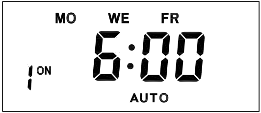
4. Set timer
Press [TIMER" button, select and set timer. Setting rotation : 1on, 1off, 2on, 2off, ...... , 10on, 10off.
Press [HOUR" button to set hour for timer.
Press [MIN" button to set minute for timer.
Press [WEEK" button to set weekday for timer. Multiple weekdays can be selected. ex: if selected [MO", the timer will only apply on every Monday; if selected [ MO, WE, FR", the timer will apply on every Monday, Wednesday and Friday.
Press [RES/RCL" button to cancel the selected on or off timer. The screen will show "-- -- : -- --" , the timer is canceled.
Press [RES/RCL" button again to reactivate the timer.

When timers are set, press [CLOCK" to quit timer setting and return to clock.
5. Random function

Press [RANDOM" button to activate random function, press again to cancel function.
System only runs random function when [AUTO" is on.
Random function will automatically start the timer from 2 to 32 minutes after the setting.
ex : if timer 1on was set to 19:30 with the random function on, the timer will activate randomly between 19:33 to 20:03.
if timer 1off was set to 23:00 with the random function on, the timer will activate randomly between 23:02 to 23:32.
To avoid overlapping, make sure to leave a minimum of 31 minutes gap between different sets of timer.
6. Manual control
Displayed features:
ON : socket turns on.
OFF : socket turns off.
AUTO : socket turns on/off automatically via timer.
Manual ON setting
Press [ON/AUTO/OFF" button to switch from [AUTO" to [ON".
This mode allows socket of the device to power up. Power indicator will light up.
Manual OFF setting
Press [ON/AUTO/OFF" button to switch from [AUTO" to [OFF".
This mode turns socket of the device off. Power indicators will turn off.
7. Electrical parameters
Operating voltage : 230VAC
Battery : NiMh 1.2V
Power consumption : < 0.9W
Response time : 1 minute
Power output : 230VAC/16A/3680W
Q&A
Q: Why won`t my timer turn on?
A: It`s out of battery, you can charge the timer by plugging onto any power outlet. Charge the device for at least 15 minutes. Then press [RESET " button to reset the device.
Q: Can I set seconds of the timer?
A: No, the smallest time unit is minute.
Q: Does my timer keeps old settings without being plugged onto a power outlet?
A: Yes, the timer has an internal battery, it allows the timer to save settings without a power outlet.
Q: Is the battery rechargeable?
A: Yes, the battery is rechargeable. We recommend to charge it for 4 hours so the battery is fully charged.
Q: Does the timer needs internet connection?
A: The timer does not need internet.
Q: Does the screen have back light function?
A: It doesn`t support back light.
Digital Timer Socket, Timing Switch Socket, Electronic Timer Socket, Timer Socket
NINGBO COWELL ELECTRONICS & TECHNOLOGY CO., LTD , https://www.cowellsockets.com