This article introduces the design of the integral arithmetic circuit.
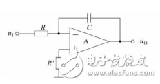
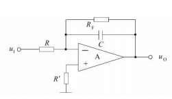
Characteristic Analysis of Integral Operation CircuitThe following figure shows the basic inverting integral operation circuit with integrated operational amplifier as the core component. The input voltage uI is applied to the inverting input terminal of the operational amplifier via the resistor R. C is the feedback capacitor, and the voltage is connected in parallel with negative feedback. R' is the balance resistor. , uO is the output voltage.
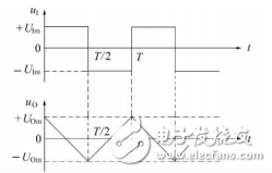
When the input signal uI is a rectangular wave with a duty ratio of q=50%, an amplitude of ±Um, and a period of T, the output signal is a triangular waveform, and the input and output signal waveforms are as shown in the following figure.
The circuit principle is analyzed as follows. The circuit equation is established by the virtual short and virtual break of the ideal op amp and the virtual ground concept of the circuit.
The general representation of the integral operation relation for solving equation (1) is
Circuit time constant

When the integral circuit enters the steady state, the initial voltage on the capacitor C is not zero. For convenience, the integrated analysis of the circuit during 0≤t≤T is discussed. During the period from 0 to T/2, the input signal uI=UIm and the initial voltage on the capacitor C are +UOm, which is obtained by the equation (2).
It can be known from equation (7) that by selecting the value of the time constant RC, the amplitude UOm of the output voltage and the amplitude of the input voltage are one of UOm>UIm, UOm=UIm, and UOm<UIm3. Since the maximum output voltage of the integrated operational amplifier is a finite value close to the supply voltage ±VCC, the amplitude UOm of the output voltage of the integral operation circuit satisfies

Inverting integral operation circuit input resistance
In order to prevent integral saturation or cut-off caused by integral drift, a resistor RF is often connected to the circuit (below).
Integral operation circuit for preventing integral saturation or cutoff
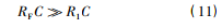
However, access to the RF will cause a shunt of the charge and discharge current of the capacitor, resulting in an integral error. In order to reduce the error, it should generally be satisfied.
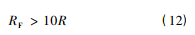
Usually selected
The design of the inverting integral operation circuit is the frequency or period T of the rectangular signal with the input terminal input duty ratio of 50%, the amplitude ± UIm, the amplitude of the output voltage ± UOm and the input resistance RI, and the RC integration circuit is determined. Component parameters. The design steps are:
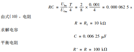
The time constant of the circuit is determined by equation (8), the resistance R is determined by equation (9), and the value of capacitor C is solved.
Design example: design an inverse integral operation circuit. The frequency of the input rectangular wave signal is f=1kHz, the amplitude UIm=±2V, the amplitude of the output voltage UOm=±8V, the input resistance RI=10kΩ, the op amp The power supply voltage is ±VCC=±12V.
The design process is as follows.
UOm = ±8V, ±VCC = ±12V, which satisfies the linear operating condition of equation (9).
From equation (8), the time constant of the circuit
The Multisim10 simulation software performs simulation analysis and verification on the designed inverting integral operation circuit [7, 8]. The simulation circuit constructed is shown in the figure below. The input signal uI is a rectangular wave with a duty ratio of q=50%, amplitude UIm=±2V, frequency f=1kHz (period T=0.001s), and the dual-track oscilloscope is used to observe the input signal uI and the voltage across the capacitor uC. Waveform.
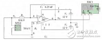
Integral operation simulation circuit
The simulation waveform is as shown in the figure below, in which the waveform of the input rectangular wave signal uI and the voltage across the capacitor uO are sequentially from top to bottom. Move the two cursor pointers at the peak-to-peak position of the waveform of the voltage uO. The peak-to-peak value of the output voltage can be read as 15.727V, and the amplitude of the output voltage is UOm=15.727V/2=7.8635V. The output voltage value of the small theoretical design can be corrected by appropriately reducing the capacity of the capacitor C. As can be seen from Figure 5, the output voltage waveform is a linear waveform with better linearity.
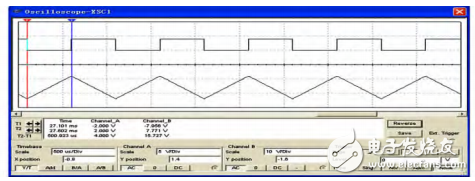
Simulation waveform of integral operation circuit
12 Woofer Speaker,Woofer Speaker 12 Inch,12 Inch Woofer Speaker,Pro Audio Tweeter Speaker
Guangzhou Yuehang Audio Technology Co., Ltd , https://www.yhspeakers.com