A voltage-controlled high-power current source design scheme based on cascade PID control algorithm is proposed. The current source adopts a PID control circuit in the inner loop circuit to improve the current response speed; the outer loop circuit adopts a digital PID control algorithm to accurately control the cascade PID control mode of the current output. Compared with the traditional current source, the current source has the advantages of large output power, output of multiple different waveform currents, large adjustable amplitude range, short pulse current rise time, and the like, and has better versatility.
introduction
High-power current sources have a wide range of applications in semiconductor laser technology, LED lighting technology and national defense technology. At the same time, high output requirements are imposed on the output characteristics of current sources, and the current output current accuracy of high-power current sources developed in China. And the stability is poor, the power is small, the frequency amplitude adjustment is poor, the pulse current rise time is long, the pulse width can be adjusted in a small range, and the efficiency is low. There are many uses of current sources, and the voltage-controlled current source is widely used due to its simple design and convenient debugging [1].
The voltage-controlled high-power current source based on the cascade PID control algorithm proposed in this paper has large output power, can output multiple different waveform currents, and has wide adjustable amplitude range, short pulse current rise time and adjustable pulse width. It has a wide range of advantages, and has good versatility, which can meet the requirements of most technical fields. The user can freely select or set the desired current waveform. The signal generation module in the control unit calls the desired waveform data in the waveform database, and the signal conditioning circuit and the automatic gain control circuit in the peripheral circuit perform conditioning and amplification, and the high-power current occurs. The circuit outputs power after amplifying the desired waveform.
Overall design
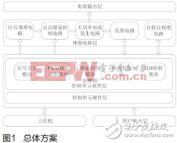
The system consists of user input layer, control unit hardware layer, control unit software layer, peripheral circuit layer, current output layer and upper computer. It can output four pulse currents, square wave current, sine wave current and arbitrary wave of no more than 20A. Current, as shown in Figure 1. The user can select or set the desired waveform by the user input layer, and the desired waveform data in the waveform database is called by the signal generation module in the software layer of the control unit, and is adjusted and amplified by the signal conditioning circuit and the automatic gain control circuit in the peripheral circuit layer. The high-power current generating circuit power-amplifies the desired waveform and inputs it to the current output layer. The user can also set at the user input level to set the frequency and amplitude of the desired waveform to meet the needs of different users. The system is designed to design a serial communication module such as USB/RS232, which is convenient for the user to input the output current data and waveform into the host computer; the user can also input the waveform data to the control unit through the USB/RS232 interface using an external storage device (such as a USB flash drive). In this way, the current of an arbitrary waveform can be obtained. The PID control circuit is adopted in the peripheral circuit layer, and the cascade PID control algorithm is adopted to accurately control the current output, quickly adjust the amplitude frequency of the output waveform, and shorten the rise time of the pulse and the square wave current.
Establishment of current source control model
The cascade PID control system [2] is one of the effective methods to improve the quality of control, and has been widely used in process control. The so-called cascade control uses two PID controllers to work in series. The output of the outer loop PID controller is used as the set value of the inner loop PID controller. The output of the inner loop PID controller controls the actuator, so that the outer loop is Control has a better control effect. In order to obtain high-precision, high-stability current output, a high-power current source based on cascade PID control algorithm is designed. The control model is shown in Figure 2.
There are two PID controllers in the control model, PID2 is the inner loop controller, the loop surrounding PID2 is called the inner loop PID control loop, and the output control quantity u1 of the outer loop controller PID1 is used as the external reference value of PID2, and PID1 In the given state, the loop surrounding PID1 is called the outer loop PID control loop.
The control sequence of the cascade PID control system is the first outer loop PID control loop (PID1) and the rear inner loop PID control loop (PID2). There are two control modes: one is asynchronous sampling control, that is, the sampling control period T1 of the outer loop PID control loop is an integer multiple of the sampling control period T2 of the inner loop PID control loop, because it is the outer loop control object in the general cascade control system. The response speed is slow and the response of the inner loop control object is fast. The other is the same-frequency sampling control, that is, the sampling control period of the internal and external PID control loops is the same. At this time, since the response speed of the controlled object of the inner loop circuit is fast, the sampling period should be selected according to the inner loop loop.

Technical route and part of the circuit principle
Technical route
According to the control model of the current source, the technical route of the system is designed. As shown in Fig. 3, the control unit controls the output of four signals, and the user input waveform parameters can adjust the waveform frequency, wherein the two paths are pulse wave and square wave signal, respectively. After the high-frequency clutter is removed by the shaping circuit, the automatic gain circuit is controlled by the control unit according to the waveform parameter input by the user, and the amplitude of the waveform is adjusted to obtain a stable and accurate pulse waveform and a square wave waveform signal. A square wave signal generated by the control unit is subjected to a sine wave waveform signal through a D/A conversion circuit, and a high-order harmonic generated by D/A conversion is filtered through an active low-pass filter (LPF) circuit, and then the automatic gain is controlled. The circuit adjusts the amplitude of the waveform to obtain a stable and accurate sine wave and arbitrary waveform signal. The four signals outputted by the control unit are modulated and amplified and input to the large current generating circuit. The large current generating circuit is composed of a high-power driving tube and a feedback circuit, and the four signals are boosted into a large current and output by the output interface, and a large current occurs. The circuit adopts analog PID control technology and adopts cascade PID control algorithm to automatically adjust the current output value to improve accuracy and stability. The current source is designed to design a serial communication module such as USB/RS232, which is convenient for the user to input the output current data and waveform into the host computer; the user can also input the waveform data to the control through the USB/RS232 interface using an external storage device (such as a USB flash drive). The unit, and then through the signal conditioning amplifier circuit, high-power current generation circuit, can obtain the current of arbitrary waveform. The self-test self-calibration module is designed in this current source to let the user know whether the system is normal before use. At the same time, the system is automatically calibrated to improve the current output accuracy. The system uses the display module to display the output current waveform and data to establish a friendly human-computer interaction interface.
Circuit principle based on inner loop PID control
The basic principle of the inner loop PID controller is applied to the current source design, and the constant current source circuit of the single high power MOS tube based on the analog PID control is obtained as shown in Fig. 4.
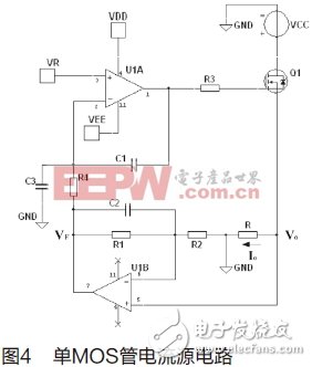
In Figure 4:
VR is the control voltage;
Vo is the feedback voltage;
VCC is the supply voltage;
Io is the constant current of the output;
U1A, U1B are high speed operational amplifiers;
R is the sampling resistor.
The specific circuit analysis is as follows:
The reference voltage VR is connected to the non-inverting terminal of the operational amplifier U1A, and the operational amplifier U1B controls the conduction level of the transconductance amplifier, and thereby obtains a corresponding output current, and the output current generates a sampling voltage on the sampling resistor R, and the sampling voltage passes through the U1B amplifier. After being fed back to the inverting input terminal of the voltage amplifier U1A as a feedback voltage, and compared with the voltage of the non-inverting input terminal, the output voltage is adjusted to adjust the output current of the transconductance amplifier, so that the entire closed-loop feedback system is dynamically balanced. In order to achieve a stable output current. Using the definition of virtual short, imaginary and related formulas, the relationship between VR and Io can be derived:

Self-test self-calibration module circuit principle
The main task of the self-test is to detect whether some key devices in the system are faulty and can work properly. After the system parameters are initialized, the self-test flow is entered. The control unit sends data to the network communication module, and determines whether the communication module is normal by detecting whether the feedback data is consistent with the transmitted data. Collect the electrical signals of each sensor to determine whether the sensor is present and can work normally. If a fault is found, the corresponding fault message is given on the display.
This current source uses self-calibration technology to improve measurement accuracy and reliability. Self-calibration techniques include external calibration and internal calibration. In this current source, external calibration mainly refers to the application of zero drift automatic calibration. Zero drift is one of the main causes of zero error. When the input signal is zero, the output signal is not zero, and the zero drift value changes with temperature. The current source uses a low temperature drift, good stability test sensor and conditioning circuit module device, which greatly reduces the impact of temperature changes on the device test. Assuming that the zero drift voltage is Vos, the calibration zero drift voltage is Vos, and the calibration circuit principle is shown in Figure 5.
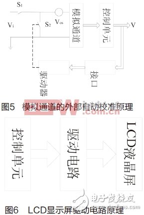
External calibration is divided into the following three steps:
(1) The switch S1 is cut off, and the switch S2 is closed, that is, the analog input channel is connected to the ground under the control of the control unit, and the output value N0 of the A/D conversion in this case is obtained;
![]()
Where K is the total amplification factor.
(2) S2 is cut off under the control of the control unit, S1 is closed, and the measured signal Vi and the drift voltage Vos are sent together into the analog channel; at this time, the output value of an A/D conversion obtained is:
![]()
The above two measurement data are calculated by the control unit:
![]()
After the calculation, the output value is N, which eliminates the influence of the zero-drift voltage Vos and truly represents the output value of the output voltage Vi.
Internal calibration technology refers to calibration with a higher-precision sensor. This current source uses a set of higher-precision sensors of the same model to generate a set of calibration values ​​for the same current, which is pre-stored in the external memory as a calibration table. The measurement data is interpolated in the corresponding calibration table to obtain the correct value after error correction, which significantly improves the measurement accuracy.
Display drive circuit principle
The current source is intended to use an LCD liquid crystal screen as a display module, and the output pulse current value is displayed on the LCD screen in the form of waveforms and data to realize human-computer interaction, so that the user can see at a glance. The driving ability of the general control chip is relatively weak, the driving voltage is low, and the excitation of the LCD display [3] requires a large current. Therefore, the level matching circuit and the driving circuit are required to improve the driving capability of the control chip. Figure 6 is a schematic diagram of the LCD display driver circuit.
System software design
As shown in Figure 7, it is a system software flow chart. After the system is powered on, the control chip is reset, and the system is initialized. After the system is finished, the system performs self-test. If the detection system is abnormal, the fault is prompted by the display module. Otherwise, the waveform setting interface is entered, and the user can select and select according to the needs. Set the desired waveform, the system will automatically load the waveform data from the waveform database according to the parameters set by the user, and then automatically detect the actual output current value through the system, and compare it with the current value set by the user. If the difference between the set value and the measured value Within a certain range ±C, it is considered to be an accurate value. The waveform and data of the measured value are displayed through the display module. Otherwise, the system will automatically adjust the frequency or amplitude of the current according to the parameters input by the user to meet the requirements of the user.

Conclusion
The high-power voltage-controlled current source based on cascade PID control designed in this paper has large output power, can output multiple different waveform currents, and has wide adjustable amplitude range, short pulse current rise time and adjustable pulse width. Great advantages, good versatility, can meet the requirements of most technical fields.
USB 2.0 Hub
Another version of USB HUB.When comparing 2.0 and 3.0 there are a few major differences. First the transfer rates: USB 2.0 offers transfer rates of 480 Mbps and USB 3.0 offers transfer rates of 4.8 Gbps - that's 10 times faster. Note that the transfer speeds also depend on the device in use in addition to the bus type and USB ports and cables.

USB 2.0 Hub,Macbook Usb Hub,Macbook Pro Hub,Hub for Laptop
Pogo Technology International Ltd , https://www.wisesir.net