With the passage of time, the integrated circuit industry has developed to this day, and there is an advanced foundry like Intel, which proposes a plan to enter the 10 nm process. The implementation of high integration has also made the chip scale larger and larger, the function is more and more complex, and the design difficulty is getting higher and higher [1]. The complication of the internal clock of the SOC has led to an increasing number of interfaces across the clock domain. In response to the processing of these asynchronous signals, foreign pioneers have put forward many constructive opinions. However, there are many devices generally used. Considering the cost factor, small-scale ICs cannot be tolerated, and if the input pulse high level is lower than the fastest clock cycle, it is generally not applicable. Therefore, in order to solve this problem well, we must deal with four aspects: one is how to simplify the circuit; the second is how to adapt to the minimum input pulse width; the third is to solve the metastable problem; the fourth is to improve the design reliability. Sex [2].
1 Common methods for processing signals across clock domains
In actual use, there is often a case where the signal is transmitted in the clock domain where the frequency is not used. For this case, two methods are generally used: the knot method and the effective control signal method. When a signal enters another clock domain from one clock domain, a metastable problem often occurs [4]. Metastability means that the trigger cannot reach an identifiable state within a specified period of time. When a flip-flop enters a metastable state, it is impossible to predict the output level of the cell or predict when the output will stabilize at a certain level. The purpose of signal synchronization is to prevent the upper metastable state from adversely affecting the next stage. The signal synchronizer should be designed by means of signal synchronization. There are three main types of signal synchronizers: level synchronizer, edge detection synchronizer, and pulse synchronizer [7-8]. However, these common methods have their own shortcomings and incompatibility. In solving practical problems, specific solutions need to be designed according to specific situations.
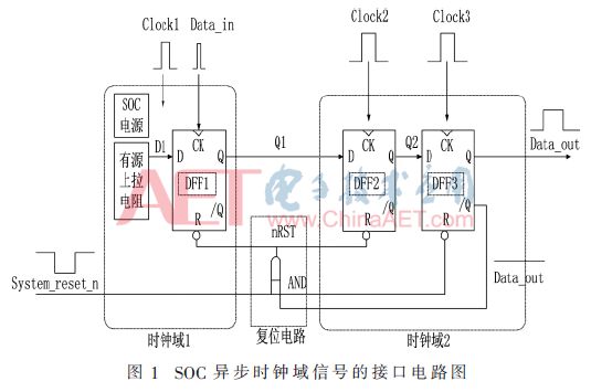
2 Cross-clock domain synchronization circuit interface method composition and working principle
The entire circuit includes two clock domains and a reset circuit. Clock domain 1 contains a synchronous trigger with an asynchronous reset. The flip-flop has an asynchronous reset terminal R and a synchronous clock terminal CK. The low level generates a reset, and the rising edge of the clock starts to latch the state of the data input terminal D. The output has two kinds of data output: normal phase Q, inverting / Q. The clock domain 2 is composed of two identical flip-flops, and is composed of an asynchronous reset terminal R and a synchronous clock terminal CK and a data input terminal D as before. The output terminal is positive phase Q, inverting / Q. The reset circuit consists of an AND gate and receives the data of the reverse/Q output of DFF3. The circuit connection relationship is shown in Figure 1.
3 Cross-clock domain synchronization circuit operating characteristics
In the design, the leak-free signal is guaranteed to the utmost. At the same time, the input pulse signal width (high level width) of clock domain 1 can be lower than the clock single period width of clock domain 1, the circuit works normally, and the pulse width in the design is no longer limited by the clock frequency of clock domain 1. Third, the pulse signal width outputted by the data output terminal Q of the data latch is clock cycle 2 clock cycle width, thereby avoiding false triggering and multi-triggering.
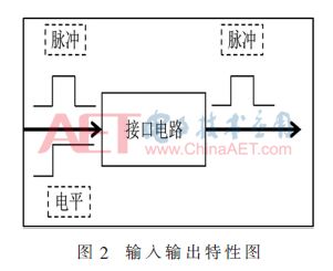
This method is suitable for input signal types of pulses or levels, and the final result is a pulse. as shown in picture 2.
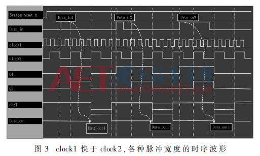
As shown in Figure 3, when clock1 is faster than clock2, Data_in1 in the figure indicates the first input pulse. This pulse is input by Data_in. The pulse width is less than a quarter of clock1. At the same time, the pulse width is smaller than the fastest clock of the system (clock1). The fastest one quarter. At the moment when the rising edge of Data_in1 arrives, Q1 outputs a high level "1"; after the rising edge of Data_in1, the rising edge of the first clock2 arrives at an instant, Q2 outputs a high level "1"; the rising edge of the second clock2 comes. At the same time, Data_out outputs a high level "1". At the same time, nRST generates a reset signal, resets DFF1, DFF2, and makes Q1 and Q2 output low. The rising edge of the third clock2 arrives at an instant, since Q1 and Q2 have already become low. Level "0", at this time, "0" is passed to Data_out, forming a pulse of data_out1 of clock2.
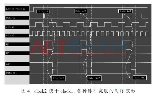
As shown in Figure 4, if clock2 is faster than clock1, Data_in1 in the figure indicates the first input pulse. This pulse is input by Data_in. The pulse width is less than a quarter of clock1. At the same time, the pulse width is smaller than the fastest clock of the system (clock2). The fastest one quarter.
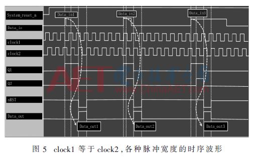
As shown in Figure 5, when clock2 is equal to clock1, Data_in1 in the figure indicates the first input pulse. This pulse is input by Data_in. The pulse width is less than a quarter of clock1. At the same time, the pulse width is smaller than the fastest clock of the system (clock2 is equal to A quarter of clock1).
4 Simulation experiment analysis
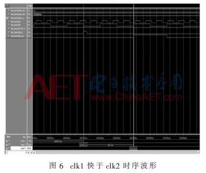
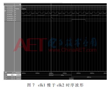
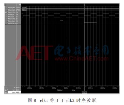
According to the above analysis, the following time domain images can be verified by Modelsim simulation analysis. As shown in Fig. 6 to Fig. 8, the fast clock is 10 Hz, the slow clock is 3.3 Hz, and the clock is equal to 5 Hz. From the simulation image, the metastable problem and the signal width are limited by the clock width problem.
5 Application and measurement
Below is an example of a design process based on Hejian Technology's 180 nm Pflash production process. The solution is based on Faraday 0.18 m m GII Library Standard Cell, and the gray part of the figure is the analog IP. In the output interface of the SAR_ADC in the figure below, there is a pulse signal whose width is equal to half of the system clock period. Using a general approach, this pulse cannot be captured, and the circuit described above effectively solves this problem. The specific implementation running code is as follows:
Assign ADC_fine_rst = ADC_fine_sys || rst ;
% generates the reset signal ADC_fine_rst, which is active high. In order to reset the ADC_fine_sys and rst high level, a “logical OR†operation is used.
Always @(posedge drdy_dig or posedge ADC_fine_rst )
If (ADC_fine_rst)
ADC_fine <= 1'b0;
Else
ADC_fine <= 1'b1;
% corresponds to DFF1 in Figure 1, drdy_dig is the original narrow pulse signal, if it is directly sampled by the system clock clk_system, it will not be latched. Therefore, here drdy_dig is connected to the clk side of ADC_fine_reg. Drdy_dig is the output signal of the ADC's IP circuit, synchronous logic output, effectively suppressing glitch and avoid false triggering.
Always @(posedge clk_system or posedge ADC_fine_sys )
If (ADC_fine_sys)
ADC_fine_ff <= 1'b0;
Else
Begin
If (rst)
ADC_fine_ff <= 1'b0;
Else
ADC_fine_ff <= ADC_fine;
End
% corresponds to DFF2 in Figure 1, where the synchronous reset logic of rst is not decisive and can be removed.
Always @(posedge clk_system or posedge rst )
If (rst)
ADC_fine_sys <= 1'b0;
Else
ADC_fine_sys <= ADC_fine_ff;
% corresponds to DFF3 in Figure 1, and the ADC_fine_sys signal is generated from the original drdy_dig signal, thereby achieving cross-clock docking.
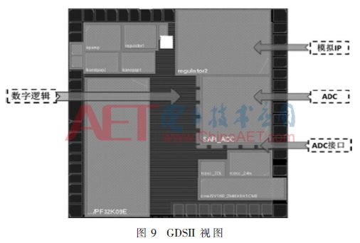
Finally, a GDSII view as shown in FIG. 9 is generated. The test board shown in Figure 10 is made according to the generated GDSII view.
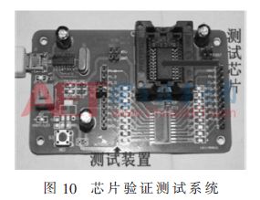
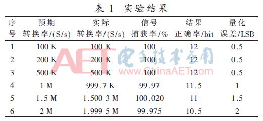
After the MPW shuttle and full MASK, the SOP20 packaging process of Tianshui Huatian was used, and the board-level test system was designed. The results of the special test SAR_ADC are shown in Table 1. The performance of the ADC is in accordance with the spec, eliminating the influence of the test environment, the signal acquisition success rate is equal to 100%, and the interface circuit scheme is successful.
6 Conclusion
Overall, the method is simple in structure. The input pulse signal width can be lower than the clock cycle width of the clock itself, so that the pulse width in the design is no longer limited by the clock frequency; meanwhile, the input pulse signal width in the clock domain 1 can be lower than the system clock cycle single cycle width, further Improve the stability and adaptability of the acquisition. The clock domain 2 output pulse signal width is clock cycle 2 clock single cycle width, thus avoiding false triggering, the circuit is synchronized through two stages, which solves the metastable problem well. Overall, the stability and adaptability of the acquisition is improved.
However, this processing method also requires input signals: the input glitch width should be less than the minimum clock recognition of DFF1 (as shown in Figure 3), otherwise false triggering will occur. Therefore, the input signal of this method is generally the output signal of the SOC synchronization circuit. If the input is an off-chip signal, the pre-digital filter circuit is generally added.
Metro Energy Feedback Transformer
Metro Energy Feedback Transformer,Dry-Type Power Transformer,Scb Power Transformer,Energy Feedback Transformer
SANON DOTRANSÂ Co., Ltd. , https://www.sntctransformer.com