Inductorless switching regulator
Previously inductor-based switching regulators (SRs) were considered to be the best power supply architecture. However, for low-power and high-integration electronic systems, SR based on embedded inductors has multiple constraints, and these constraints can be overcome with a non-inductive architecture. Based on the implementation cost (BOM and pin count) and performance (efficiency, noise and reliability), this article provides the magnitude and quantitative comparison for the above two architectures.
Implementation cost and BOM list
The first and most important constraint of an inductor-based regulator (Figure 1) is cost and inductor size. In most cases, inductors dominate the cost and size of integrated SR. To solve this problem, consumer product designers who are responsible for cost budgets try to choose cheap inductors with large power consumption, but this will reduce power efficiency. For example, if an inexpensive inductor is used in an inductor-based SR instead of a low ESR (equivalent series resistance) inductor, it will lose up to 10% efficiency. Therefore, the advantages of inductor-based SR will no longer exist.
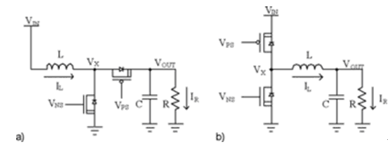
Figure 1: Common inductor-based boost (a) buck (b switching regulator.
On the other hand, the non-inductive SR (Figure 2) only needs to use one or two small and inexpensive ceramic capacitors (flying capacitors Cf1 and Cf2) to replace expensive inductors. In fact, for a given output capacitor, the cost of the inductor is about 5-10 times that of the flying capacitor, and the volume ratio has reached 5-10 times or even higher.
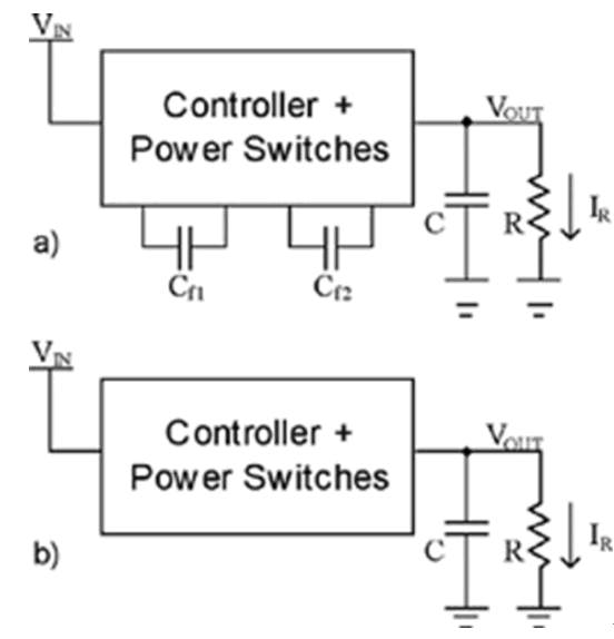
Figure 2: Ordinary non-inductive switching regulator (a), ordinary non-inductive switching regulator with flying capacitor (b).
At low current (<25mA), the flying capacitor can even be integrated into the silicon chip, thus providing extremely high integration for high-efficiency integrated conversion. At this time, the regulator only needs an external output capacitor.
Many published materials on integrated SRs using embedded inductors have clearly stated that this type of SR requires very high switching frequencies, which ultimately fall out of people ’s attention because of low efficiency and silicon The large chip size also requires RF technology.
It should also be noted that in order to ensure the stability and optimal performance of the regulation loop, external components are usually required to compensate for the conjugate pole formed by the LC filter (inductor and output capacitor). In the non-inductive regulator, no compensation is required, thereby reducing the cost of passive components.
The number of pins required may be the main problem in the non-inductive solution. It can be seen from Figures 1 and 2 that the inductor-based SR requires 4 pins (VIN, VOUT, VX, and GND), while the non-inductive SR requires 3-7 pins (VIN, VOUT, Cf11, Cf12, Cf21, Cf22, and GND), depending on the output current capacity and the ratio of VIN to VOUT.
As also mentioned above, external passive components are required in an inductive solution, which usually requires 2 additional pins.
In total, the inductive solution requires 4-6 pins, while the non-inductive solution requires 3-7 pins.
Performance and efficiency
Inductive SR, also known as a charge pump (Figure 2), is known to be less efficient than inductive solutions when the input voltage is variable. But since the development of multi-mode non-sense SR products, the above statement is no longer true. This solution provides an average efficiency similar to inductive SR in the general battery voltage range.
Indeed, in charge pump converters, multiple topologies can be used to achieve different conversion ratios. For example, for a non-inductive SR with 2 flying capacitors and different switching modes, 11 voltage conversion ratios can be achieved: 4/1, 3/1, 2/1, 3/2, 4/3, 1, 3 / 4, 2/3, 1/2, 1/3 and 1/4. Now it is possible to realize a non-inductive SR that automatically selects between all these conversion ratios. The efficiency is:
It can be found by monitoring VIN and VOUT that SR will automatically select the appropriate conversion ratio to achieve the highest efficiency according to the VIN / VOUT operating point. For example, Figure 3 shows the efficiency curve of a non-inductive SR with two flying capacitors in the input voltage range of 2.6-5.5V and for two different output voltage values.
It can be seen that this type of SR can achieve an average efficiency of more than 80% over the entire input voltage range, which is obviously in the same range as the efficiency that can be achieved with inductive solutions. Similarly, for fixed conversion ratios such as VIN = 5V and VOUT = 3.3V (USB power line to I / O or analog voltage field), the efficiency can be as high as 85%.
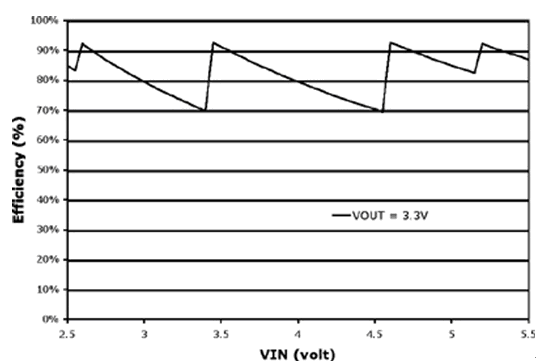
Figure 3: The relationship between efficiency and input voltage in a non-inductive switching regulator.
Since there are multiple operation modes in the portable electronic system, the current consumption of the system and different sub-modules varies greatly. The SR powering these submodules must achieve high efficiency over a wide current range. Therefore, another important aspect of efficiency is how it responds to changes in SR load current. Most inductive SRs use a PWM adjustment loop. This scheme can achieve high efficiency when the load is heaviest, but its efficiency drops rapidly when the load is reduced.
Figure 4 shows the dependence of efficiency on load current in PWM inductive SR. It can be seen from the figure that the efficiency drops rapidly at light load. In order to maintain efficiency at lighter loads, inductive SRs usually use solutions that consume less energy, such as PFM or PSM (pulse frequency hopping modulation). However, the disadvantage of this type of modulation scheme is that it seriously reduces the adjustment performance of the SR and also greatly increases the inherent output noise.
Figure 4 also shows the effect of the inductor's ESR on the maximum achievable efficiency. In order to truly achieve the efficiency stated in the data sheet of the inductive SR provider, an ultra-low ESR inductor must be used, but such an inductor is always large and expensive. In fact, due to cost constraints, system or production engineers are often looking for cheap inductors. Therefore, the average efficiency of the inductive SR in the higher current output range (10% -100% of IOUT) is often between 80% and 85%, as shown in Figure 4. In fact, the average efficiency of the inductive scheme has been reduced to that of the small and cheap ceramic capacitors in the non-inductive SR scheme. Even if cheap inductors are used, their size and cost are not worthwhile. degree.
Non-inductive SR will have the same efficiency loss under light load. However, products such as DOLPHIN's SRO-2.6 ~ 5.5 / 1/8 ~ 3.3 adopt an innovative adjustment scheme to reduce the power loss of SR as the load is reduced, and at the same time can maintain the efficiency at the best-that is 99% at full load, without any loss of adjustment performance and noise performance.

Figure 4: The relationship between the efficiency of the PWM inductive SR (a) and DOLPHIN SRO-2.6 ~ 5.5 / 1.8 ~ 3.3 non-inductive SR (b) and the load. The working conditions are VIN = 3.3V & VOUT = 1.8V. Previously inductor-based switching regulators (SRs) were considered to be the best power supply architecture. However, for low-power and high-integration electronic systems, SR based on embedded inductors has multiple constraints, and these constraints can be overcome with a non-inductive architecture. Based on the implementation cost (BOM and pin count) and performance (efficiency, noise and reliability), this article provides the magnitude and quantitative comparison for the above two architectures.
Implementation cost and BOM list
The first and most important constraint of an inductor-based regulator (Figure 1) is cost and inductor size. In most cases, inductors dominate the cost and size of integrated SR. To solve this problem, consumer product designers who are responsible for cost budgets try to choose cheap inductors with large power consumption, but this will reduce power efficiency. For example, if an inexpensive inductor is used in an inductor-based SR instead of a low ESR (equivalent series resistance) inductor, it will lose up to 10% efficiency. Therefore, the advantages of inductor-based SR will no longer exist.
Figure 1: Common inductor-based boost (a) buck (b switching regulator.
On the other hand, the non-inductive SR (Figure 2) only needs to use one or two small and inexpensive ceramic capacitors (flying capacitors Cf1 and Cf2) to replace expensive inductors. In fact, for a given output capacitor, the cost of the inductor is about 5-10 times that of the flying capacitor, and the volume ratio has reached 5-10 times or even higher.
Figure 2: Ordinary non-inductive switching regulator (a), ordinary non-inductive switching regulator with flying capacitor (b).
At low current (<25mA), the flying capacitor can even be integrated into the silicon chip, thus providing extremely high integration for high-efficiency integrated conversion. At this time, the regulator only needs an external output capacitor.
Many published materials on integrated SRs using embedded inductors have clearly stated that this type of SR requires very high switching frequencies, which ultimately fall out of people ’s attention because of low efficiency and silicon The large chip size also requires RF technology.
It should also be noted that in order to ensure the stability and optimal performance of the regulation loop, external components are usually required to compensate for the conjugate pole formed by the LC filter (inductor and output capacitor). In the non-inductive regulator, no compensation is required, thereby reducing the cost of passive components.
The number of pins required may be the main problem in the non-inductive solution. It can be seen from Figures 1 and 2 that the inductor-based SR requires 4 pins (VIN, VOUT, VX, and GND), while the non-inductive SR requires 3-7 pins (VIN, VOUT, Cf11, Cf12, Cf21, Cf22, and GND), depending on the output current capacity and the ratio of VIN to VOUT.
As also mentioned above, external passive components are required in an inductive solution, which usually requires 2 additional pins.
In total, the inductive solution requires 4-6 pins, while the non-inductive solution requires 3-7 pins.
Performance and efficiency
Inductive SR, also known as a charge pump (Figure 2), is known to be less efficient than inductive solutions when the input voltage is variable. But since the development of multi-mode non-sense SR products, the above statement is no longer true. This solution provides an average efficiency similar to inductive SR in the general battery voltage range.
Indeed, in charge pump converters, multiple topologies can be used to achieve different conversion ratios. For example, for a non-inductive SR with 2 flying capacitors and different switching modes, 11 voltage conversion ratios can be achieved: 4/1, 3/1, 2/1, 3/2, 4/3, 1, 3 / 4, 2/3, 1/2, 1/3 and 1/4. Now it is possible to realize a non-inductive SR that automatically selects between all these conversion ratios. The efficiency is:
It can be found by monitoring VIN and VOUT that SR will automatically select the appropriate conversion ratio to achieve the highest efficiency according to the VIN / VOUT operating point. For example, Figure 3 shows the efficiency curve of a non-inductive SR with two flying capacitors in the input voltage range of 2.6-5.5V and for two different output voltage values.
It can be seen that this type of SR can achieve an average efficiency of more than 80% over the entire input voltage range, which is obviously in the same range as the efficiency that can be achieved with inductive solutions. Similarly, for fixed conversion ratios such as VIN = 5V and VOUT = 3.3V (USB power line to I / O or analog voltage field), the efficiency can be as high as 85%.
Figure 3: The relationship between efficiency and input voltage in a non-inductive switching regulator.
Since there are multiple operation modes in the portable electronic system, the current consumption of the system and different sub-modules varies greatly. The SR powering these submodules must achieve high efficiency over a wide current range. Therefore, another important aspect of efficiency is how it responds to changes in SR load current. Most inductive SRs use a PWM adjustment loop. This scheme can achieve high efficiency when the load is heaviest, but its efficiency drops rapidly when the load is reduced.
Figure 4 shows the dependence of efficiency on load current in PWM inductive SR. It can be seen from the figure that the efficiency drops rapidly at light load. In order to maintain efficiency at lighter loads, inductive SRs usually use solutions that consume less energy, such as PFM or PSM (pulse frequency hopping modulation). However, the disadvantage of this type of modulation scheme is that it seriously reduces the adjustment performance of the SR and also greatly increases the inherent output noise.
Figure 4 also shows the effect of the inductor's ESR on the maximum achievable efficiency. In order to truly achieve the efficiency stated in the data sheet of the inductive SR provider, an ultra-low ESR inductor must be used, but such an inductor is always large and expensive. In fact, due to cost constraints, system or production engineers are often looking for cheap inductors. Therefore, the average efficiency of the inductive SR in the higher current output range (10% -100% of IOUT) is often between 80% and 85%, as shown in Figure 4. In fact, the average efficiency of the inductive scheme has been reduced to that of the small and cheap ceramic capacitors in the non-inductive SR scheme. Even if cheap inductors are used, their size and cost are not worthwhile. degree.
Non-inductive SR will have the same efficiency loss under light load. However, products such as DOLPHIN's SRO-2.6 ~ 5.5 / 1/8 ~ 3.3 adopt an innovative adjustment scheme to reduce the power loss of SR as the load is reduced, and at the same time can maintain the efficiency at the best-that is 99% at full load, without any loss of adjustment performance and noise performance.
Figure 4: The relationship between the efficiency of the PWM inductive SR (a) and DOLPHIN SRO-2.6 ~ 5.5 / 1.8 ~ 3.3 non-inductive SR (b) and the load. The working conditions are VIN = 3.3V & VOUT = 1.8V.
In summary, Figures 3 and 4 clearly show that when selecting SR according to efficiency, further consideration should be given to the achievable efficiency under maximum load conditions, and with the different operating conditions (VIN, VOUT, IOUT) in the system Efficiency changes.
An important application criterion is the acceptable noise of the SoC circuit power supply. The voltage source provided by the regulator has two sources of contribution: one is the noise coupled from the regulator input to the output, which is called PSSR (Power Supply Rejection Ratio), and the other is the inherent noise of the regulator itself. As long as the regulator has sufficient bandwidth and open-loop gain, both inductive and non-inductive SR can achieve very high PSSR. However, the inherent noise of the switching characteristic of these regulators (generated by the regulator itself) becomes the dominant noise. Therefore, the first choice is to select the SR with the lowest inherent noise.
Figure 5 shows the inherent noise of inductive and inductive switching regulators (including flicker noise and thermal noise and output ripple). Both of these structures present higher noise on the switching frequency fsw and its harmonics. If the SR load is sensitive to certain frequencies, the SR switching frequency must be outside this sensitive frequency range.
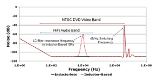
Figure 5: Output noise characteristics of inductive SR.
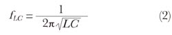
For the inductive SR, additional noise is distributed near the resonance frequency of the LC filter composed of the inductor and the output capacitor. The frequency is:
The L and C values ​​required in many portable applications will form an LC filter, and usually its resonant frequency will fall within the audio or video range. As shown in Figure 5, the noise amplitude of such LC tank circuits usually exceeds the SR white noise, which will change the performance of sensitive analog loads such as audio amplifiers.
Reducing the amplitude of the inherent noise of the switch can be achieved by increasing the output capacitance value. However, this will move the resonance frequency of the LC filter deeper into the sensitive audio band.
Substrate noise
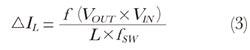
Current ripple is the peak-to-peak value of the current flowing through the inductor (Figure 7) and is defined as:
Why do people want to reduce current ripple? There are three main reasons: to reduce the output voltage ripple, to reduce the injection of substrate charge, and to maintain the best efficiency in a larger output current range.
The first reason is quite clear, because the output voltage ripple of the inductive SR is proportional to the current ripple flowing through the inductor.
To understand the second reason, you need to review the basic principles of inductive SR. For simplicity, we use inductive buck SR as an example. But note that the concepts discussed here are also applicable to inductive boost SR. It can be divided into two categories (Figure 6): asynchronous (a) and synchronous (b) regulators (there are some other types derived from these two categories, but this does not belong to the scope of this article). The main difference between these two types of SR lies in the usage of the diode, not the usage of the switch. In the asynchronous scheme,
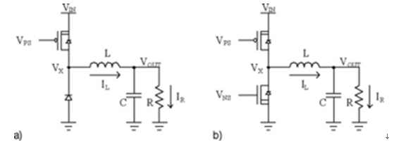
Figure 6: Asynchronous (a) and synchronous (b) inductive switching regulators.
Asynchronous SR has a major advantage, which is relatively simple, but because diodes dissipate a lot of power, high efficiency cannot be achieved. On the other hand, to achieve high efficiency with synchronous SR, the two switches must not be turned on at the same time. Therefore, non-overlapping circuits must be used.
During the non-overlapping period, both switches are off, and the current flowing through the inductor establishes a potential between the two switching patterns (VX in 6b), which will activate the body diode of the switch and The current is directly injected into the substrate. This will produce substrate noise, and when the wiring of SR is not good, it will increase the probability of occurrence of latch-up. Obviously, the greater the current ripple, the greater the transient noise injected into the substrate, which will cause a lot of ground noise. In addition, it is extremely difficult to evaluate or simulate the impact of such noise on the converter and even the entire system.
The only way to eliminate this problem and potentially dangerous state is to add an external low Vth Schottky diode to Vx. The diode will be activated before the body diode of the switch, thereby eliminating substrate current injection. But this will increase the BOM cost, and this problem is already a fatal flaw of inductive SR.
On the other hand, in the non-inductive SR, the only source of noise injected into the substrate is generated through the coupling of parasitic capacitance. Therefore, the substrate noise generated by the inductive SR will not be higher than the noise generated by any digital circuit of the same size operating at the same clock frequency. In terms of substrate noise, integrating a non-inductive SR is no more dangerous than integrating a CMOS logic block.
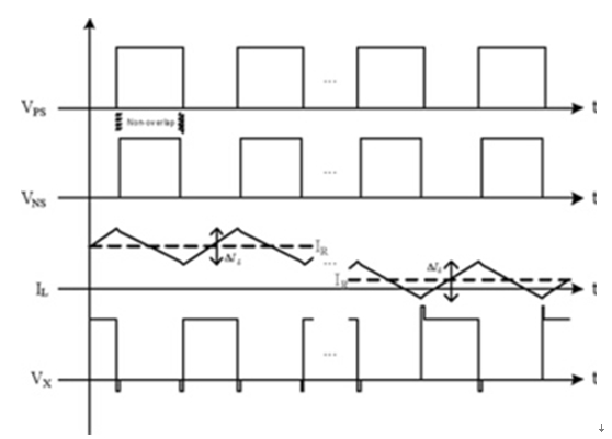
Figure 7: Characteristics of synchronous switching regulators.
Duty cycle harmonic diffusion noise
Inductive SR uses a PWM loop for regulation. This means that the output voltage ripple duty cycle will vary with operating conditions. Therefore, harmonic distortion is not well defined, it will change with VIN, VOUT, and IR. The non-inductive SR is not controlled by PWM, but uses linear adjustment, so it can always maintain a stable 50% duty cycle at the output.
EMI noise
Another inconvenience of using inductive SR is its potential EMI, which will occur with other parts of the system. There are switched inductors on the PCB, which basically radiate electromagnetic waves of the frequency spectrum shown in Figure 5. Sensitive RF or analog circuit performance will greatly change this electromagnetic phenomenon, and it is also extremely difficult to predict or simulate.
SR may also be a victim of other sources of electromagnetic interference, because these sources will couple noise to VOUT through inductors. This is another source of noise that is difficult to predict and simulate.
These EMI problems can be solved by shielded inductors, but unfortunately this has to increase costs, shielded inductors are more expensive than unshielded ones.
reliability
As shown in Figure 7, the potential energy at node VX may reach VIN + Vth or -Vth. This will generate high voltages, leading to long-term reliability problems. When the power supply voltage of SR is higher than the voltage specified by the process technology (such as 4.2V lithium battery), the situation will be worse. And this 'over-voltage' problem will not exist in the non-inductive SR, so it will have higher voltage reliability, or easier protection.
in conclusion
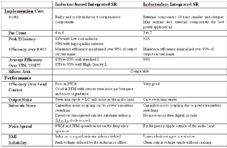
The following table summarizes the advantages and disadvantages of inductive and non-inductive integrated SR used in portable electronic systems with low power consumption and high integration.
In conclusion, we firmly believe that inductive switching regulators will provide a more cost-effective solution that can replace traditional inductive switching regulators and be integrated into SoCs used in portable consumer electronics devices.
Trolley Plastic Speaker:
Our hot selling products: Trolley Plastic Speaker. You can also call it outdoor dancing speaker, Portable Karaoke Speaker. Trolley Plastic speaker has plastic enclosure, stylish, small, portable and compact. It built in trolley handle and wheels Wireless outdoor stereo speaker with TF/USB/MP3. You can use it enjoy webcast, movie, music, and also you can use it to accompany when you dance. Especially it is a mini Karaoke systems, you can sing everywhere if you like, it can bring you unexpected happiness. We are looking forward to establish win-win business relationships with you. Warm welcome you to our company and introduction this trolley speaker systems to you!


Trolley Plastic Speaker
Trolley Plastic Speaker,Trolley Speaker Systems,Trolley Speaker With Wifi,Trolley Speaker With Led Screen
Shenzhen New Wonderful Technology Co., Ltd. , https://www.sznewwonderful.com