Current output DS1862 XFP laser control and digital diagnostic IC has two current outputs. BIASSET is an analog current DAC output with a maximum output of 1.5mA. MODSET is an 8-bit current DAC with 1.2mA full scale. For this application, the voltage range of these DAC outputs should be between 0.7V and 3.0V.
Current-voltage conversion Here, an operational amplifier is used to convert the BIASSET and MODSET current DAC into a voltage output with a differential amplifier configuration structure. In addition to generating a voltage output, the circuit in Figure 1 can effectively disable the DS1862's built-in APC loop by pulling current directly from the BMD pin. The circuit in Figure 2 converts the MODSET DAC to a voltage output with a full-scale range of 1.09V.
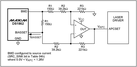
Figure 1. BIASSET current-voltage conversion circuit
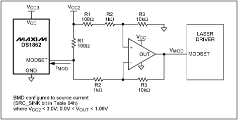
Figure 2. MODSET current-voltage conversion circuit
The compact solution uses chip-scale packaged operational amplifiers and 0201 resistors to provide the most compact solution. The MAX4233 is a two-channel operational amplifier, available in a 1.5mm x 2mm, 10-ball UCSP â„¢ package.
APCSET voltage calculation The output voltage of the op amp in Figure 1 is calculated using equations 1 and 2. Two DS1862 registers (APCc <7: 0> and APCf <1: 0>) adjust the current flowing into the BIASSET pin.


Using the values ​​given in Figure 1, when the DAC current is 1.5mA, the maximum input voltage of APCSET is 1.26V.
The BMD output has an output impedance of up to 700Ω. In Figure 1, R1 should be less than 180Ω to ensure that the voltage at the DAC pin is not lower than 0.7V.
To produce a stable output voltage, the leakage current flowing into the differential amplifier should be minimized. In Figure 1, R2 >> R1 must be guaranteed to keep the ratio of the current flowing into the differential amplifier to the current flowing out of the BMD pin to a minimum. Since 39.2kΩ is more than 200 times larger than 150Ω, it can meet the above requirements. To further reduce offset and gain errors, a resistor with a 1% tolerance should be selected.
MODSET voltage calculation The output voltage of the operational amplifier shown in Figure 2 is calculated using Equation 3.

Using the values ​​shown in Figure 2, the maximum input voltage of MODSET is 1.09V. In order to reduce the offset and gain errors, a 1% tolerance resistor should be used. At the same time, the selected R1 should ensure that the voltage at the DAC pin is not lower than 0.7V. If VCC2 is 1.8V, R1 <825Ω should be selected.
A compact solution using chip-scale packaged operational amplifiers and 0201 resistors will provide the most compact solution. The MAX4233 is a dual operational amplifier in a 1.5mm x 2mm, 10-ball UCSP package, which is ideal for this application.
Tx power monitoring considers that some applications require monitoring of Tx power. This cannot be achieved using the circuit in Figure 1, because BIASSET must be connected to the BMD through a resistor. When the BMD is connected in this way, the monitor diode of the laser will not be connected to the DS1862. Therefore, other devices must be used to provide voltage to the APCSET pin of the laser driver.
The circuit in Figure 3 shows an implementation method. This circuit uses the DS1855 digital potentiometer to set the voltage of the APCSET pin of the laser driver. Pin H0 of DS1855 is connected to the voltage reference (VREF) of the laser driver. In this circuit, the monitor diode of the laser can be connected to the BMD pin of the DS1862 and can be in sink or source mode.
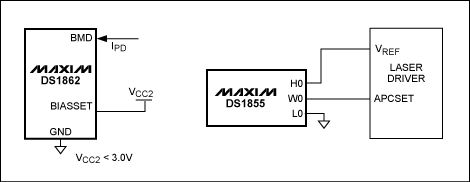
Figure 3. BIASSET current-voltage conversion circuit
Conclusion A small and simple circuit can be used to convert the current output of the DS1862 to a voltage output. If you need Tx power monitoring, you can choose to use the DS1855 digital potentiometer combined with the reference output of the laser driver.
Surface-mount technology (SMT) is a method for producing electronic circuits in which the components are mounted or placed directly onto the surface of printed circuit boards (PCBs). An electronic device so made is called a surface-mount device (SMD). In industry, it has largely replaced the through-hole technology construction method of fitting components with wire leads into holes in the Circuit Board. Both technologies can be used on the same board, with the through-hole technology used for components not suitable for surface mounting such as large transformers and heat-sinked power semiconductors.
By employing SMT, the production process speeds up, but the risk of defects also increase due to the components miniaturization and denser packing of boards. In those conditions, detection of failures has become critical for any SMT manufacturing process.[1]
An SMT component is usually smaller than its through-hole counterpart because it has either smaller leads or no leads at all. It may have short pins or leads of various styles, flat contacts, a matrix of solder balls (BGAs), or terminations on the body of the component.

Surface Mount Technology,Surface Mount,Surface Mount Assembly,Surface Mounting Technology
Orilind Limited Company , https://www.orilind.com