In the design of digital circuits, timing design is a major indicator of system performance. In the high-level design method, the abstraction of timing control is also improved accordingly, so it is difficult to grasp in the design, but in understanding the timing model of RTL circuit On the basis of reasonable design method, it is effective in designing complex digital systems. It is proved by many design examples that the post-simulation pass rate of the circuit can be greatly improved and the operating frequency of the system can reach a higher level. .
1 Several basic concepts in digital circuit design:1.1 Establishing time and holding time:
The setup time (setup TIme) refers to the time when the data is stable until the rising edge of the trigger's clock signal arrives. If the setup time is not enough, the data will not be triggered into the trigger on the rising edge of this clock; hold time (hold TIme) ) refers to the time when the data is stable after the rising edge of the trigger's clock signal. If the hold time is not enough, the data cannot be triggered into the trigger. Figure 1 . The stable transmission of data must meet the setup and hold time requirements, although in some cases the setup and hold times can be zero. The PLD/FPGA development software can automatically calculate the setup and hold times of two related inputs (Figure 2).
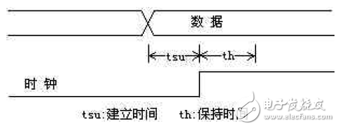
Figure 1 Relationship between setup time and hold time
Note: When considering the establishment of hold time, the clock tree should be considered to be skewed backwards. When considering the setup time, the clock tree should be considered to be skewed forward. In post-simulation, the maximum delay is used to check the settling time and the minimum delay is used to check the hold time.
The settling time constraint is related to the clock cycle. When the system fails to operate under the high frequency clock, lowering the clock frequency allows the system to complete its work. The hold time is a parameter that is independent of the clock cycle. If the design is unreasonable, the place and route tool cannot provide a high-quality clock tree. Therefore, the clock frequency cannot be adjusted anyway, only the system is modified. It is possible to work normally, resulting in greatly reduced design efficiency. Therefore, the timing of a reasonable design system is the key to improving the quality of the design. In programmable devices, the skew of the clock tree can be ignored, so the hold time is usually satisfied.
1.2 Competition and risk phenomena in FPGASignals have a certain delay when they are connected and logic cells inside the FPGA device. The size of the delay is related to the length of the connection and the number of logic cells, and is also affected by the manufacturing process, operating voltage, temperature and other conditions of the device. The high and low transitions of the signal also require a certain transition time. Due to the two factors, when the level value of the multi-channel signal changes, at the moment of signal change, the output of the combinatorial logic has a sequence, not simultaneously, and some incorrect spike signals often appear. These spike signals Called "burr". If a "glitch" appears in a combinatorial logic circuit, it means that the circuit is "adventurous." (Unlike discrete components, since there is no parasitic capacitance inductance inside the PLD, these spurs will be completely retained and transferred to the next stage, so the glitch is particularly prominent in PLD and FPGA design.) Figure 2 is an example of a logical adventure. It can be seen from the simulation waveform of FIG. 3 that after the four input signals of "A, B, C, D" are subjected to the wiring delay, the high-low level conversion does not occur at the same time, which causes the output signal "OUT" to have a glitch. (We can't guarantee that the lengths of all the connections are the same, so even if the four input signals change at the same time on the input, the time to reach the OR gate is different through the internal routing of the PLD, and the glitch must be generated). In a nutshell, as long as the input signal changes at the same time, the combinatorial logic will produce glitch (through the internal trace). The design method of connecting their outputs directly to the clock input, clearing or setting the port is wrong, which can have serious consequences. So we have to check all glitch-sensitive input ports such as clock, clear and set in the design to make sure the input does not contain any spurs.
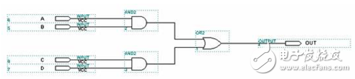
Figure 2 Example of a circuit with logic adventure
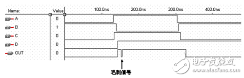
The simulated waveform of the circuit shown in Figure 3.
Adventures often affect the stability of logic circuits. Clock ports, clear and set ports are very sensitive to glitch signals, and any glitch can cause system errors, so judging whether there is an adventure in the logic and how to avoid risk is a problem that designers must consider.
How to deal with burrsWe can reduce the occurrence of burrs by changing the design and destroying the conditions created by the burrs. For example, in digital circuit design, the Gray code counter is often used to replace the ordinary binary counter. This is because the output of the Gray code counter has only one bit transition at a time, which eliminates the occurrence of competitive risk and avoids the occurrence of glitch.
Glitch is not harmful to all inputs. For example, the D input of the D flip-flop, as long as the glitch does not appear on the rising edge of the clock and meets the data setup and hold time, it will not cause harm to the system. We can say D The D input of the trigger is not sensitive to the glitch. According to this characteristic, we should use the synchronous circuit as much as possible in the system. This is because the change of the synchronous circuit signal occurs at the clock edge. As long as the glitch does not appear at the edge of the clock and does not satisfy the data setup and hold time, it does not. It can cause harm to the system. (Because the glitch is very short, mostly a few nanoseconds, it is basically impossible to meet the data establishment and retention time).
LiFePO4 Batteries Replace Lead-acid Battery
Likewise, too slow of a charge of lead acid batteries can cause premature sulphation, shortening their life. This is not a problem with lithium.
- Lead acid batteries tend to perform best between C/8 and C/12 rates. So our 100Ah battery would want to be charged or discharged at between 8A and 12A. Wiring three batteries in parallel would permit three times the rate, as it shares the current between the three, so 24A to 36A.
- Some lithium batteries can generally handle a C/1 rate, or even higher for short periods depending on the battery. This means a 100Ah lithium battery can handle 100A (or more) of charge/discharge current. Most manufacturers recommend no more than a C/2 rate on a regular basis for best battery life, but it is good to know the extra power is there with lithium batteries if you need it. Be sure to check the manufacturer`s specs when selecting a lithium battery, as some do not support as high of a current as others.
-

-
IT`S TIME TO MOBILIZE WITH LITHIUM BATTERIES FOR MARINE AND RV APPLICATIONS
Whether you are looking for a new battery bank for your RV or boat or considering replacing your aging lead acid batteries, deep-cycle lithium ion batteries – specifically LiFePO4 batteries – are an excellent solution. Compared to lead acid batteries, LiFePO4 batteries offer more power, higher current, a longer life, smaller footprint, lower weight, and safe, maintenance-free operation. Are you ready to mobilize and go lithium?
Lithium Phosphate Battery,Lithium Ferro Phosphate Battery,Replace Lead-Acid Battery,Fortune Lifepo4 Battery Cells
Shenzhen Sunbeam New Energy Co., Ltd , https://www.sunbeambattery.com