Analog design is never easy. Engineers can spend their entire careers on phase-locked loops (PLLs), because for them to be correct, it requires an in-depth understanding of the function of the circuit, including their response to different process boundaries and different manufacturing processes.
In the age of FinFET, these challenges are intensifying in analog circuits. For example, reuse is a common practice in digital design, but it has not been applied to multiple nodes in analog design, because analog circuit scaling cannot exceed a certain limit.
Technically, there are several reasons for this situation. Mick Tegethoff, Director of Product Marketing and Management, Analog / Mixed Signal Verification, Siemens Mentor, said: "High-precision analog designers will not be satisfied with reuse and migration because, for example, there are no tools in analog technology that guarantee timing closure. We Seeing that traditional analog designers spend a lot of time to really understand the function of the design. "
More and more physical and electrostatic effects appearing in the FinFET node force the engineering team to use migration as an option, and reconsider the architecture, design the circuit, and conduct more verification at the same time.
Tegethoff said: “What drives all this is smaller geometric patterns, which actually contain some features that are helpful for analog design. In a sense, analog device miniaturization will improve effects such as leakage current, Its miniaturization is not like a digital device. This is not the kind of thing that can be done by miniaturization. Some things do make it more difficult. For high-precision ADCs, PLLs, and precision analog circuits, when you move to more advanced The random noise of the device itself will become the main factor that can not be ignored, which needs to be considered in the simulation. "
For the two types of noise that are on transistors — thermal noise and flicker noise — transient noise analysis can be run within SPICEsimulation. “This is a time-domain analysis, but at every time step it inserts the random noise for each of the devices , "Tegethoff said." And while it does make stimulation take longer, design teams can simulate complex PLLs or high precision ADCs in the time domain to see it locking, see its stability.
For two types of noise on transistors-thermal noise and flicker noise, transient noise analysis can be run in SPICE simulations. Tegethoff said: "This is a time domain analysis, but every step inserts random noise for each device. Although it does make the simulation take longer, the design team can simulate a complex PLL or high precision in the time domain. ADC to observe its lock or stability. "
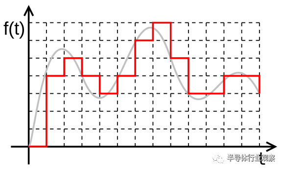
Figure 1: Digital and analog signals. (Source: Wikipedia)
Another growing challenge involves interconnection resistance, which is getting worse on every new node. For interconnection, the resistance and capacitance of the interconnection itself must be considered in the simulation of the circuit. Otherwise it will be inaccurate. The thinner the conductor, the greater the resistance.
Tegethoff said: "If the output of a transistor is connected to another transistor, then in the past, you can think of it as an ideal wire with zero resistance. Now it has a certain resistance, which means that after the circuit layout, The layout parasitic parameters must be extracted. These must be fed back to the schematic and simulated again with all the content. This will cause the number of components on the circuit to increase by 100,000 times and the simulation time will be much longer. If you use resistors Carry out the simulation and find that it does not meet the specifications, then you must go back, change the content and simulate again-not to mention the need for additional verification. "
In analog IP, other factors that drive complexity include the variability of the device itself, which requires Monte Carlo-type analysis to ensure that the variability is controllable. The behavioral characteristics of the device depend on the layout content and environment, and this is usually caused by the layout dependence effect (LDE). Muthu Vairavan, senior product marketing manager for Cadence Design IP, said these effects significantly increase the iteration between design and layout.
Vairavan said: "In addition, due to complex design rules, the use of multiple exposures to print these low-level geometric patterns increases the usual layout period. Analog designers also need to consider the mismatch effects related to line edge roughness and these low-level feature sizes. Interconnect changes. The advent of FinFETs has placed additional constraints on analog designs because device widths must now be discrete multiples of fins (unlike planar transistors). These devices are also susceptible to manufacturing changes in fin width and height, As well as the effects of vias and interconnect resistance, this complicates analog matching. "
Although analog designers and tool vendors have adopted new design methods and tool flows to adapt to these changes, each node brings new complexity, leading to cost and time-to-market challenges. Vairavan pointed out: "A growing trend seen in high-performance enterprise applications is the shift from SoC to system-in-package (SiP) design, where multiple analog and digital chips are integrated in the package. This allows digital design to be transferred to Advanced nodes to achieve product differentiation, but still use proven analog IP from old nodes. This is due to the advancement of multi-chip modules and 2.5D integration technology, as well as the increase in the availability of interconnects in high-bandwidth, low-power packages . "
However, for low-cost system applications, the challenges still exist, and the increase in cost of package-level integration is unreasonable. Vairavan added: "Even in high-performance data centers and cloud applications, key mixed-signal designs, such as very high-speed DSP-based SerDes, will benefit from higher density and lower power advanced nodes. Therefore, analog design People need to continue to innovate, and foundry manufacturers and tool suppliers need to add analog design feedback to the early process and tool development cycle of analog design to alleviate these challenges. Analog IP is a key difference in many SoC designs, their performance and quality It is critical to the success of these products. "
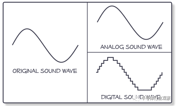
Figure 2: Not everything can be digitized (Source: Center Point Audio)
Node and foundry challenges
The process migration of analog circuits has always been tricky, but in the field of FinFET, it has become a bigger problem.
Ed Petrus, ArterisIP technical consultant explained: "Because of the challenges faced by advanced nodes, the old technology that people call migration is more or less similar to compression. For example, in existing layouts, the PLL of older nodes such as 350nm will increase A multiplier factor of 0.X. For analog circuits, this has always been a problem, because analog circuits have very strict requirements for matching such design techniques. When there are two wires in and out of a certain differential circuit, these two The current of the root wire must match. This is achieved by placing the device very strictly in this circuit. The problem with old-style compression is that, because it is an algorithm, it does not understand these strict requirements. In the analog world, These are called constraints. These matching requirements will eventually be unknowingly destroyed by compression. Therefore, the final circuit will not work properly. "
This problem has existed since 180nm. Below this, everything needs to be redesigned.
Petrus said: "The characteristics of the device have changed a lot. The designer must re-examine the circuit and determine whether the existing type of circuit is really suitable for the new node. If it can work, then the topology will be maintained and the device size will be maintained. It will be adjusted, which is usually sufficient. But for advanced nodes, this is unlikely, so the design team will eventually return to the circuit and redesign most of the content. "
Advanced process nodes were not created at all considering the simulation characteristics. They were developed to reduce the area of ​​digital circuits.
Manuel Mota, product marketing manager at Synopsys, said: "The reality is that analog circuits and analog interfaces will eventually need to be integrated into digital modules. Of course, those who design these modules and those who want to integrate them do face challenges. This can be solved. of."
These challenges stem from the inherent characteristics of the process. Mota said: "Some of these effects have even begun to appear in high-volume processes, and the impact of using FinFETs will be more obvious. Moreover, these devices themselves are much more complicated, and their modeling has become more complicated and more difficult to use. Features no longer depend on the direct proximity of the internal device. Now, proximity effects have far exceeded the usual effects, and designers can no longer assume certain characteristics of transistors to design. It must be assumed that it is in a In a large circuit, you must consider all these effects around. This applies not only to the device, but also to the connection around the device. So connecting one device to another device is also quite complicated. "
Even if metal stacks are used, they can be considered almost ideal in the past, but now resistance, capacitance, and parasitics play an important role in the characteristics of the entire circuit design. In addition, there are effects related to FinFET.
Mota said: "You can no longer arbitrarily design the gate width and gate length you want. In the past, this was possible. The significance of this for analog design is that, first of all, the process usually has fewer features for analog design, so it is There are more uncertainties in the electrical characteristics of. The rules you have to follow and verify are much more complicated, and verification design becomes more time-consuming, and can be easily increased by 3 or 4 times in advanced nodes. "
In addition, in the past, in very conservative electrical simulation nodes (such as aging and reliability), some design-insensitive things are now critical, especially in the automotive, medical, and industrial applications.
Mota said: "You need to design them and verify everything. This extends the design cycle again. And in terms of simulation, if you are dealing with the fine evolution of voltage and current during simulation, this may mean very long verification Period. This is one of the main challenges. Then, when it comes to the characteristics of processes and devices, they are not necessarily ideal for analog design. Assuming you have a digital-centric device, its analog characteristics are very poor. . Maybe they are poorly modeled from a simulation point of view, and these are usually not solved by modern analog design. Traditional technology cannot solve the problem of creating a linear design. To some extent, you are doing exactly On the contrary, you have to admit that this process is not good, you have to accept the characteristics of this process and the characteristics of the transistor you are designing are not very good. What you do is to take advantage of the advantages of this process, such as rich devices. In this process, You can have millions of doors, which are basically free and can be calibrated. "
Tegethoff said: “Given all this, the trade-off is a delicate balance. If you have knowledge about the circuit and do migrate, then sometimes you have to adjust the circuit. The more verification you run, the more simulations you run, and the sense of variability you run The more variability-aware simulation, the smaller the margin you have, and abnormal phenomena will not occur. Unfortunately, in simulation, a large part of the margin is area or power. In order to reduce the impact of noise , You need to increase the power and other things. Finally, the model of the device itself is more complicated. The equation of the FinFET device model will be 3 or 4 times more. "
The problem of simulating IP in advanced nodes ultimately comes down to everything becoming more and more complicated, and the third-order effect becomes the first-order effect. Tegethoff said: "The end result is that we continue to require accurate SPICE simulations on these nodes, including longer simulations, more simulations, and the need for intelligent environments. For example, Monte Carlo simulation continues to require accurate circuit simulations, but It needs to become faster and handle larger circuits so that they can complete their work within a reasonable time. "
in conclusion
Looking to the future, designers still need to go all out to solve all this, considering the frequency and bandwidth required to support technologies such as 5G. This is extremely complex and will become more complicated.
Tegethoff said: "Analog content is becoming more and more important because they are on the border. Whether it is the Internet of Things, communications or cars, you must deal with the analog world. These interfaces need to be faster, they need to be accurate, and need to be low. Power consumption. "
The art of analog design, which was once a bit isolated, now has to deal with many of the same problems as advanced digital design, and there are some unique problems with analog circuits.
PCB Mount Type current sensing transformer
A Current Transformer (CT) is a type of transformer that is used to measure alternating current (AC). It produces a current in its secondary which is proportional to the current in its primary.
Current transformers, along with voltage or potential transformers, are instrument transformers. Instrument transformers scale the large values of voltage or current to small, standardized values that are easy to handle for measuring instruments and protective relays. The instrument transformers isolate measurement or protection circuits from the high voltage of the primary system. A current transformer provides a secondary current that is accurately proportional to the current flowing in its primary. The current transformer presents a negligible load to the primary circuit.

Product name
PCB Mount Type current sensing transformer
Smart meter, Energy monitoring devices
1.Low profile, compact size, Epoxy resin encapsulated, fully enclosed.
2. PCB mounting type, easy to fix and install.
3.wide linearity range for output current and low phase shift error.
4.Customer specifications are available.
5. Used in universal and be in good interchangeability.
Brand name
Magason-tech
Model Number
ZCT02 series
Usage
Coil Structure
Toroidal
Phase
Single
Material
core, wire, resin , plastic case
Certification
ISO9001:2015, ROHS
Package
Carton
Shipping Term
DHL Fedex TNT EMS UPS
Product features


 We attend Electrical exhibition In India, Germany and Brizil, South Korea...
 All of our material meet the RoHs, UL , SGS, CE certification
FAQ
1-MOQ?
We will work hard to fit your MOQ .Small purchase quantity is ok.
2-Payment term?
T/T, Western Union, Paypal, Credit Card
3-Delivery port?
Shenzhen, Guangzhou, Zhongshan, Hongkong.
4-Shipping date?
About 7 days when we check the payment.
5-Do you produce the core and bobbin by yourself .
Yes.we have 2 head company,1 subsidiary company.one is bobbin factory,one is core factory,last one is transformer factory.
6-Where is your factory?
In ShaanxI
Mini Pcb Current Transformer,Pcb Current Transformer,Energy Meter Current Transformer,Precision Pcb Current Transformer
Shaanxi Magason-tech Electronics Co.,Ltd , https://www.magason-tech.com