As cities attach importance to street lighting, the workload of management, monitoring, control and maintenance of street lighting has increased, and the problem of limited human and material resources has become increasingly prominent. In order to improve the efficiency of street lamp management, a new type of street lamp remote monitoring system is needed. From the current technical conditions and the comprehensive cost of communication distance, real-time, reliability and security, the remote monitoring system based on the public telephone network (PSTN) is more suitable. Therefore, for the situation of outdated equipment, poor reliability, limited equipment, low investment, many failures, many lines, and inconvenient management and maintenance in the street lamp management office, the PSTN communication method was selected, and the design and development of the intelligent street lamp controller based on AT89S8252 was conducted on the running status of city street lamps Remote intelligent monitoring.
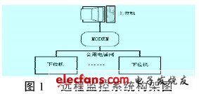
The intelligent street lamp controller is the main component of the system. It is related to the information interaction between the host computer and the street lamp controller, and is the hub of system information exchange. The intelligent street lamp controller can not only play the role of uploading and releasing, but also can control the street lamps separately. It uses PSTN communication with the host computer to complete the transmission of the controller's operating data. This can not only achieve long-distance communication, but also save line costs. The control is finer. The system architecture is shown in Figure 1.
2 Intelligent street light controller hardware circuit design and functional description
2.1 Measuring circuit
In the measurement circuit, the sampling circuit needs to collect three-phase voltage signals and four-phase current signals (including neutral current). This system uses DC sampling method. The voltage change circuit is shown in Figure 2.
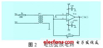
In Figure 2, PT1 is a current-type voltage transformer. The input voltage of phase A passes through the current limiting resistor R1 (100K), so that the rated current of PT1 primary (primary side) is 2.
2mA, the secondary (secondary side) will produce the same current. Through the operational amplifier (LF353), the user can obtain the required voltage output at the output by adjusting the value of the feedback resistor R3. Taking the standard power frequency voltage 220V as an example, the effective value of the converted A-phase voltage can be calculated as: the converted voltage signal meets the input voltage requirements of each component.
The current conversion circuit uses precision current transformer CTY205A (CT1), and the current change circuit is shown in Figure 3.
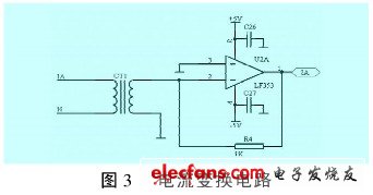
Through the operation amplifier (LF353), the user can adjust the value of the feedback resistor R4 to get the required voltage output at the output. Taking the current (AC value AC) 5A as an example, the current signal converted by the current transformer is: The converted current signal meets the input voltage requirements of each component of the system.
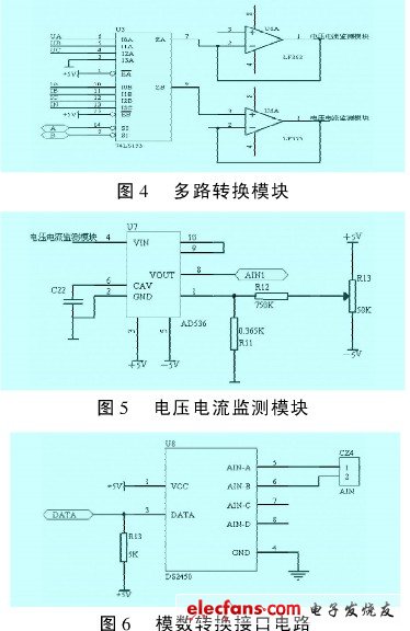
The voltage and current are transformed by a transformer and input into a double four-choice decoder. The microprocessor multiplexes by controlling the voltage and current values. LF353 is selected to be connected as an emitter follower, which plays the role of isolation and following. The multiplex conversion module is shown in Figure 4. The voltage and current monitoring module selects the effective value conversion chip AD536 to calculate the root mean square value of the input complex AC value AC, and outputs an equivalent DC value DC. Then enter the ADC conversion circuit in the system. The voltage and current monitoring module is shown in Figure 5.
The two signals collected by the voltage and current monitoring module need to be converted into the controller after being converted by the analog-to-digital converter, so the DS2450 analog-to-digital conversion interface chip is selected. DS2450 is a one-wire 4-channel successive approximation A / D converter produced by DALLAS. Its input voltage range, conversion accuracy digits, and alarm threshold voltage are programmable; each channel has its own memory to store voltage range settings and conversion results , Threshold voltage and other parameters; serial communication rate up to 16.3kbps in normal mode, up to 142kbps during over-speed operation, on-chip 16-bit cyclic redundancy check code generator can be used to detect the correctness of communication; DS2450 uses 8-pin SOIC The small size package can be powered by a single 5V power supply or a parasitic power supply. The circuit consumes only 2.5mW of power during normal operation and 25 μW when not in operation. The CPU only needs one port line to communicate with many one-line chips, occupies less ports of the microprocessor, and can save a lot of leads and logic circuits. The analog-to-digital conversion interface circuit is shown in Figure 6.
Small computer system interface (SCSI) is an independent processor standard for system level interfaces between computers and intelligent devices (hard disks, floppy drives, optical drives, printers, scanners, etc.). SCSI is an intelligent universal interface standard.
In addition to SCSI, IDE is also a very common interface. From the point of view of ease of use, IDE is more suitable for ordinary users. In addition, personal computer users not only need to configure a few peripherals, but also do not require high speed. Therefore, it is more appropriate to choose IDE interface. In addition, IDE also has the characteristics of high performance price ratio and wide application. Although the SCSI interface has many incomparable characteristics, the price of the interface and its peripherals is too expensive to be borne by ordinary users, which determines the limitation of its actual use range.
1. The working mode of IDE requires the whole process participation of CPU. When the CPU reads and writes data, it can't perform other operations. In this case, in the multitask operating system of Windows 95 / NT, the system reaction will be greatly slowed down. The SCSI interface controls the data reading and writing operation completely through the independent high-speed SCSI card, so the CPU does not have to waste time to wait, which obviously can improve the overall performance of the system. However, IDE interface has also made great improvements to improve this problem. DMA mode can be used instead of PIO mode to read and write data. DMA channel is responsible for data exchange, which greatly reduces the CPU consumption. However, comparing the CPU utilization of SCSI and IDE, we can find that SCSI still has considerable advantages.
2. The scalability of SCSI is larger than that of IDE. Generally, each ide system can have two IDE channels, with a total of four IDE devices. The SCSI interface can connect 7-15 devices, much more than IDE, and the cable connected is far longer than ide.
3. Although the price of SCSI device is higher, compared with IDE, the performance of SCSI is more stable, durable and reliable.
SCSI Solder Type Section
ShenZhen Antenk Electronics Co,Ltd , https://www.antenkelec.com