Abstract: At present, the traffic accident caused by lane departure on the expressway has caused huge losses, which makes the research of lane departure warning system become a hot spot in society. Based on DSP calculation and FPGA calculation, this paper constructs a vision-based lane departure warning system. In this paper, the framework structure and hardware implementation of the system are given. Based on the proposed system, the transmission, storage and processing of large-capacity data in the vision system are studied in detail. Finally, based on the constructed system, the feasibility of the system is verified by a series of typical visual processing algorithms and software algorithms applied to the decision of lane deviation.
This article refers to the address: http://
1 Introduction
Car driving is an action behavior involving three factors: driver, car, and road. The driver feels the road information through a series of physiological organs such as the eyes, and makes a series of driving decisions through the understanding and judgment of the road information and the tracking of the driving condition of the car. However, due to a series of factors such as the driver's long-term driving, carelessness and the driver's perception of the road information and the understanding of the vehicle's condition, there is a certain "blind zone", resulting in traffic accidents becoming more and more a major safety hazard in society. This paper starts from the driver, car and road, and studies a set of active safety systems that simulate the driving behavior of people to improve the driving safety of vehicles, and realize active safety technologies such as lane departure warning.
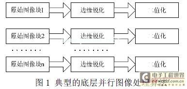
In machine vision-based systems, real-time performance has always been a major problem, especially for systems such as lane departure warning. The algorithm to be implemented covers the entire visual calculation process from image preprocessing to high-level visual computing. There are both underlying high-parallel implementations of large data volume convolution, gradation transformation and other regularization algorithms, as well as medium-level feature extraction and other pattern recognition algorithms and high-level visual processing methods to achieve understanding of the road. Wait. For a long time, the versatility and efficiency of embedded systems have always been a contradiction that is difficult to reconcile [1]. How to construct a more general vision processing system, which has higher performance for parallel and serial algorithms at all levels of vision. Implementation efficiency is a problem to be solved in this paper. The emergence of high-speed DSP processing chips and large-scale reconfigurable chips provides us with a good solution.
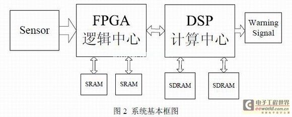
Large-scale reconfigurable chips, such as FPGAs, integrate a large-capacity look-up table-based gate system that is ideal for constructing fine-grained SIMD processing arrays or pipeline structures, as shown in Figure 2. The underlying image processing algorithm [1] has natural adaptability. TI's C6000 series of DSP computing chips, using Harvard architecture, has 8 processing units inside, and also integrates a dedicated hardware multiplier, suitable for some serial visual processing algorithms, for the higher level of data but less The computational process is more complicated, and the road has a good implementation effect.
Based on the above analysis, this paper combines high-speed DSP computing chip and reconfigurable FPGA chip to construct a high-speed embedded visual processing system. FPGA is used as auxiliary logic control and front-end processing module, mainly to complete image pre-acquisition and some similar histograms. High-density image processing at the bottom of graph statistics, convolution, etc., can be flexibly configured in hardware structure, and complete the underlying algorithm by implementing a series of parallel structures or pipeline structures to avoid resources caused by DSP to complete these fine-grained algorithms. Waste and time loss; DSP as the main computing center, complete high-level serial-based visual processing tasks, such as road understanding and interpretation, lane deviation decision, etc., DSP's high-speed processing ability can better complete these A high degree of serialization algorithm. The basic block diagram of the system is shown in Figure 2.
2, system design and implementation
To realize the vision-based automotive active safety system of Figure 2, the storage and transmission of data is a major problem, especially for the real-time requirements of automotive active safety. How to obtain the final understanding of the road and the correct decision on whether the vehicle is deflected in the shortest time, from the original captured image data, through a series of memory data movement and signal processing, The main implementation goals of the system. This article will provide a detailed introduction to the system based on the "flow" order of the data in the system.
2.1, data acquisition module
In this system, image data is the main sensor signal, and obtaining high-quality image data has great significance for later processing and function realization. However, for the actual application environment, due to the influence of weather, illumination and other factors, even a series of special situations, the general image sensor is difficult to have better robustness under various conditions. In order to better adapt to various roads and weather conditions and ensure the safety of driving, we have independently developed a visual acquisition module using a CMOS digital camera chip suitable for road use. The camera chip can be fully programmed and controlled by a 159-bit SPI control word. Better adjustment of exposure time, gain, noise, etc. is achieved. At the same time, the camera chip adopts a multi-slope exposure mode output. In different exposure modes, the exposure time is also different, ensuring that the illumination is too strong or the illumination conditions are very weak. Good image.
For the SPI control of the camera chip, in order to adaptively adjust the working mode in different backgrounds, the DSP gives the FPGA a certain communication signal to complete the system level of the top layer of the camera chip according to the final understanding and judgment of the image. Control, and the modification and adjustment of the underlying real SPI control word is done by the FPGA, which avoids the waste of DSP work efficiency caused by the inconsistency between the SPI operating frequency and the external bus frequency of the DSP, and the FPGA does the work. It is easier.
2.2, data transmission, storage module
In this system, from the image acquisition module at the front end to the output of the last alarm signal, the data is continuously transmitted and moved between FPGA, SDRAM and DSP. Next, we mainly discuss how to carry out between the three. High-speed and efficient moving and processing is the main module of this article. The data flow in the system mainly has the following aspects:
I. The preprocessed image data in the FPGA must first be stored in the main memory chip SDRAM, which is the basis for the high-end processing of the back end.
II. The DSP reads the latest image data from the SDRAM for processing, and stores the intermediate result of the processing in the SDRAM. Such a read and write process is likely to be cyclic, and the block storage characteristic of the SDRAM is suitable for such performance requirements. .
III. In order to facilitate the debugging of the system, it is very likely to display the result of the intermediate processing. Therefore, we have a display debugging module attached to the FPGA. During debugging, the FPGA can read the intermediate processing result from the SDRAM for display.
IV. There is also a case where in some cases we may require direct transfer of image data between the DSP and the FPGA, which is a category we must consider.
Combining the above possibilities, considering that our DSP chip supports the seamless connection of FIFO and SDRAM chips, we designed the data transmission scheme of Figure 3:
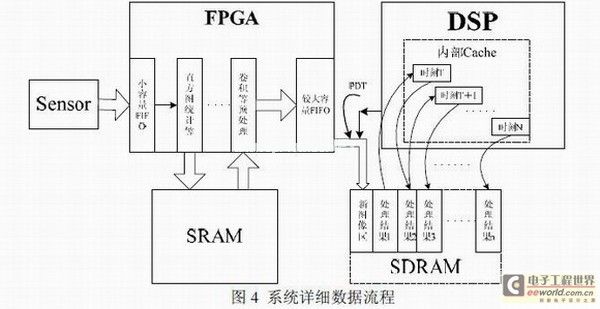
First, the image data output by the front-end acquisition module is 8-bit, and for the SDRAM memory chip and DSP processing chip we use, the data bus is 64-bit. In order not to waste resources, in the process of FPGA preprocessing the image, we simultaneously splicing 8-bit image data into 64 data output, which can make full use of the system resources.
Second, a series of parallel preprocessed image data is stored in the FIFO in the FPGA. The FPGA gives a handshake signal to inform the DSP that it can start transferring data from the FIFO to the SDRAM. The data transmission process is completely controlled by the DSP through EDMA transmission. When the core processor DSP completes the current operation, the latest data is read from the SDRAM for processing, which can make full use of the rich peripheral resources of the DSP chip.
At the same time, from the data flow diagram of Figure 3, we find that the data is transferred from the FPGA to the SDRAM. Compared with the DSP, the FIFO module and the external main memory SDRAM module developed in the FPGA to store data are attached to the DSP. On the same address bus and data bus, the DSP chip used in this type of source device and destination device is connected to the same external bus. The DSP chip supports an optimized EDMA transmission mode - PDT transmission. The data transmission process is optimized, so that the EDMA transmission mode of the DSP can be directly transmitted from the source device FIFO to the destination device SDRAM without the data being buffered in the DSP, so that the data can be transmitted in one cycle. Compared with the traditional transmission mode, the FPGA transfers to the internal buffer area of ​​the DSP, and then the DSP writes to the SDRAM. The PDT transmission mode can basically shorten the data transmission time by half, for large-capacity data transmission like images. In terms of it, it has a very big meaning.
The data migration process from the front-end pre-processing module to the main memory SDRAM is completed, followed by the high-speed data transmission process of the back end. The data transmission between DSP and SDRAM can reach a high speed rate above 100MHz, especially the EDMA transmission mode supported by DSP. It allows the transmission between external data and the Cache inside the DSP to be completed without CPU interference. This will increase the efficiency of the CPU work. In addition, there are two levels of cache inside the DSP chip, and the second level cache L2 can reach 1MB. Therefore, we consider the popular ping-pong transmission method. When the CPU is processing the ping in the cache or the data inside the pong, Under the premise that the remaining processing time can be predicted, we can transfer the data to be processed in the EDMA mode to the corresponding pong or ping storage area in advance, so that the data transmission time is included in the processing, saving The corresponding transmission time increases efficiency.
Combining the above analysis of the entire data transfer process, we can get the data transfer process shown in Figure 4. As can be seen from the figure, the data from the Sensor to the preprocessing in the FPGA, and the internal data processing of the DSP, under the buffer processing of the SDRAM, can be transferred and processed in a pipelined manner, and the FPGA acts as a front-end preprocessing module. The completion of the processing of large-capacity data has a very large effect on the improvement of system efficiency.
3, system software algorithm
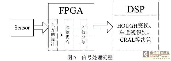
There are many introductory articles on front-end image preprocessing methods and lane departure decision-making algorithms [2][3][4]. In this paper, there is no excessive description. The main implementation process is shown in Figure 5. Through some typical algorithms in [2], we verify that the vehicle active safety system designed in this paper is fully compliant with the real-time requirements of automotive driving applications, and the system is highly scalable.
4 Conclusion
This paper introduces a set of implementation schemes of lane departure warning system based on DSP calculation and FPGA logic calculation, which mainly solves the high-speed transmission, storage and processing of large-capacity image data in the system. In the process of design, this paper makes full use of the adaptability of FPGA logic resources to the underlying visual algorithm and the high-speed processing capability of DSP chip to meet the high-level serial high visual algorithm. Through a series of experiments, it is verified that the system meets the high real-time requirements of the application of automotive safety.
This article is innovative:
(1) Combining the relationship between the driver, the car and the road environment, simulating the driving behavior of the person to design the active safety system of the car, the practical significance of the system design principle;
(2) For the adaptability of multiple levels of algorithms in computer vision system design, the combination of DSP calculation and FPGA logic calculation is adopted to meet the requirements of various levels of system algorithms;
(3) A detailed analysis of the process of data transmission, storage and processing in the computer vision system, using the optimized EDMA transmission method - PDT to meet the real-time requirements of the system;
Led Bike Lights Custom,Bike Flashlight,Led Flashlight
Thefirst International Lighting Co., Ltd. , http://www.gddivinglight.com