Long-term reliability issues, such as electronic migration (EM) failure mechanisms, have traditionally been the subject of fab processing. But as the reliability of nano-designs becomes more difficult, it's no longer a matter for designers to throw problems into manufacturing. The design world must also make an effort to obtain a more robust layout.
If the current density is too high, the metal atoms are gradually replaced, and electron migration problems occur. When too much current flows in the same direction for a long time, voids (Void, which appear when the atoms are exhausted) and hillocks (which are generated when the atoms are accumulated) begin to form on the interconnect. After enough atoms have been replaced, an open or short circuit will occur. When the hillock touches an adjacent interconnect, a short circuit occurs, causing chip failure.
One way to reduce electron migration is to extract the parasitic impedance of the interconnect and input it into a simulation tool to calculate the current flowing through each metal line. Using the width information of each part of the interconnect, it is possible to calculate the current density and classify it from low to high. A color map is then generated overlaid on the layout, thereby marking the areas with the highest current density.
First, the area with the highest current density can be processed to widen the interconnect metal lines, increase the via holes, and reduce the current density.
Once the layout has been modified, the designer can perform a parasitic impedance extraction and re-simulate the results. In this way, it should be possible to see a decrease in the current density that causes electron migration.
should:
1. Perform an EM analysis to confirm the presence of metal lines with EM problems. Parasitic impedance extraction is performed on the final layout, and the parasitic impedance value, as well as the width and position of the portion, are input to a simulation tool. The simulation generates a current density map that is overlaid on the original layout.
2. When performing parasitic impedance extraction, the variation in metal width is taken into consideration. Many fabs provide modeling mechanisms for this variation in parasitic impedance extraction.
3. Consider the thickness variation at the time of extraction. Changes in the thickness of the metal cause changes in the value of the parasitic impedance and must be taken into account.
4. Perform a simulation to calculate the current density of the entire chip layout. For each layer, the current density threshold is determined to achieve an acceptable average time to failure for the application.
5. Widening the metal wire with too high current density.
6. VIA doubling is performed on the layout to reduce parasitic impedance and thus reduce current density.
7. Perform parasitic impedance extraction, simulation, and visualization to see if the layout correction has reduced the current density in the most severe areas. If the layout correction has reduced the current density to an acceptable level, the design is complete.
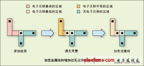
Figure 1: Widening the metal lines and adding vias to reduce current density.
Should not:
1. Missing execution of EM analysis. If it is not detected, it will cause performance degradation, which may cause chip failure in the future.
2. Throw the metal filling task to the fab. Metal filling is important to improve the flatness of the design and, if done correctly, to minimize thickness variations.
3. Perform parasitic impedance extraction without thickness and width variations. This can cause errors in the extraction, resulting in errors in current density calculations.
4. Parasitic extraction is performed by thickness calculation before adding the metal filler. The correct procedure is to first insert the metal filler and then change the width and thickness to perform the extraction.
5. Do not use double through holes. Since stress migration (Stress migraTIon) may result in less metal deposits in the vias, this increases the impedance in the poor vias and makes the current density higher.
6. Use a flat simulaTIon engine. The use of a layered architecture will greatly improve simulation time and reduce memory usage.
7. The transistor effect is ignored when calculating the current density. Since the amount of current flowing through a grid depends on parasitic parameters and related components, it is important to perform transistor-level simulations when performing EM analysis.
Ridging Machine for Agriculture:
ridging machine for Agriculture can improve the ground temperature and increase the air permeability of the soil, and our ridgers are versatile and used in farm land which is welcomed by ploughing farmers for its plurality of unique advantages. These ridging tractors are of small resistance and high efficiency. Our ridging machine also has advantages of racing against time, saving labor, working efficiency and low cost etc.

Ridging Machine for Agriculture Technical Parameters:
1. Weight: 240KG
2. Operating width: 1400 mm
3. Power: 36.8-51.8 KW
4. Size: 920*1690*1020 (mm)
Typical Applications: can be worked in paddy field, dry land, hilly ground and green house.
If you have any questions, please contact us directly. Crawler tractor for agriculture are produced by Hunan Nongfu with high quality and good appearance.
welcome you can visit our factory for inquiry, please send mail directly to us.
Ridging Machine for Agriculture
Agricultural Machinery, Ridging tractor, Ridger, ridging machine
Hunan NongFu Machinery&Electronic.Co., Ltd. , https://www.nfagmachine.com