 Xilinx Starts Filming with Ultratex's First 20nm All Programmable Device, the Industry's First ASIC-Grade Programmable Architecture, and 20nm UltraScale Devices Comparing to Competing Products, Implementing 1.5 to 2x System-Level Performance and Programmable System Integration One Year in Advance 2013 7 On the 9th, Beijing, China—Xilinx, Inc. (NASDAQ:XLNX), a global leader in All Programmable FPGAs, SoCs and 3D ICs, today announced the continuation of a series of industry innovations in the 28nm process at the 20nm process node. It once again introduced two industry firsts: the first 20nm device in the film semiconductor industry and the first 20nm All Programmable device in the Programmable Logic Device (PLD) industry; and the industry’s first UltraScaleTM ASIC programmable architecture. These first-of-its-kind industry releases continue Xilinx’s first industry-leading advantages in the 28nm field and the All Programmable SoC, All Programmable 3D IC, and SoC enhanced design suites. .
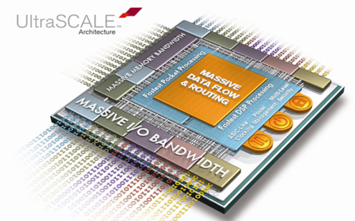
 Illustration: Xilinx UltraScale architecture: The industry's first ASIC-level programmable architecture that can scale from 20nm planar transistor processes to 16nm and even FinFET transistor technology, from monolithic to 3D IC extensions. It not only solves the problem of overall system throughput expansion limitations and latency issues, but also directly addresses the biggest bottleneck in the performance of advanced node chips - interconnection. Victor Peng, senior vice president of the Programmable Platform Products Division of Xilinx, stated: " We have developed the industry's most aggressive 20nm drop plan, and I believe that Xilinx is far ahead of the high-end devices for at least one year compared to the closest competitor, and at least mid-range devices. In about half a year, when you combine TSMC technology with our UltraScale architecture and perform collaborative optimization through our Vivado® Design Suite, we believe that we will achieve 1.5 to 2 times the system-level performance and 1 year in advance of our competitors. Programmable system integration - equivalent to a whole generation of leading competitive products."
Xilinx collaborates with TSMC to inject the high-end FPGA requirements into the 20SoC development process just like the 28HPL (high-performance, low-power) development process. Xilinx and TSMC collaborated on the 28nm process node to enable Xilinx to be the industry’s first 28nm All Programmable FPGA, SoC, and 3D IC device launcher, pushing Xilinx to cost-performance and power consumption , Programmable System Integration, and Leading Generation in Lowering Bill of Material (BOM) Costs. Xilinx has now extended this proven industry-leading collaboration model from 28nm to 20nm, introducing the industry's first ASIC-level programmable architecture, UltraScale.
The newly developed UltraScale architecture includes a 20nm planar transistor process and 16nm-to-FinFET transistor technology extensions, including monolithic and 3D ICs. It can not only solve the problem of the overall system throughput expansion limit and the problem of delay, but also can directly deal with the biggest bottleneck in the performance of advanced node chips—interconnection.
Nowadays, people need an innovative architecture to manage the system performance of hundreds of Gbps flow rates per second, and the ability to perform intelligent processing at full line rate, and can scale to Tb-class traffic and 1 billion floating-points per second Teraflop-level computing power. Simply improving the performance of each transistor or system module, or increasing the number of system modules, is not enough to achieve the above goals, so we must fundamentally improve the communication, clock, critical path and interconnect technology to achieve the industry's next-generation high-performance applications (As shown in the figure below), it meets the requirements of mass data flow and intelligent data packet, DSP or image processing.
The UltraScale architecture addresses the following challenges by adopting cutting-edge ASIC technology in a fully programmable architecture:
§ Wide buses optimized for massive data streams support multi-terabit throughput § Multi-zone ASIC-like clocks, power management, and next-generation security § Highly optimized critical paths and built-in high-speed memory cascades DSP and Packet Processing Bottlenecks § Second-generation 3D IC systems integrate step-by-step features of inter-chip bandwidth § High I/O and memory bandwidth to provide dynamic delay reduction and 3D IC wide memory-optimized interfaces § Vivado tool eliminates wiring congestion and coordination Optimized, device utilization exceeds 90% without sacrificing performance The first batch of UltraScale devices will not only expand Xilinx’s current market-leading 28nm Virtex® and Kintex® FPGAs and 3D IC product families, but will also become the future Zynq® UltraScale The foundation of All Programmable SoC. In addition, UltraScale devices will implement next-generation smarter systems with new high-performance architecture requirements, including:
§ 400G OTN providing smart packet processing and traffic management
§ 4X4 hybrid mode LTE and WCDMA Radio supporting smart beamforming
§ 4K2K and 8K displays supporting intelligent graphics enhancement and recognition § Maximum Performance System for Intelligent Surveillance and Reconnaissance (ISR) § High Performance Computing Applications for Data Center Xilinx CEO Moshe Gavrielov: “With Xilinx Industry The first 20nm product drop-in, the first ASIC-grade UltraScale architecture, the first SoC-enhanced Vivado design suite, and the continued expansion of IP, C, and ARM processor solutions supporting Smarter system design, Xilinx again Once expanded the value and market coverage of the PLD industry. At the same time, we have also competed for products in advance to bring customers a leading-edge value advantage.â€
Availability Early release versions of the Vivado Design Suite supporting UltraScale architecture FPGAs are available now. The first batch of UltraScale devices will begin shipping in the fourth quarter of 2013.
About Xilinx Xilinx is a global leader in All Programmable FPGAs, SoCs, and 3D ICs. Xilinx's industry-leading products integrate seamlessly with next-generation design environments and IP cores to meet a wide range of customer needs for programmable logic and system integration.
This is a new type of Wireless charger names Wireless Phone Charger,it`s unique design and multifunctional performance makes you safe driving without blocking sight,it`s not only a magnetic base for you to put on the mobile in case of falling down but also a wireless innovative Power Bank for charging any of QI supported mobiles.It`s Wide compatibility for many mobiles types such as Iphone,Samsung,Huawei and etc.The triangle is as stable as Mount Tai,the PC and ABS material protects your mobile from scratch or damage.You deserve this creative light Wireless Car Charger.

Wireless Phone Charger,Iphone Wireless Charger,Wireless Cell Phone Charger,Galaxy Wireless Charger
Shenzhen Hequanqingnuo Electronic Technology Co., Ltd. , https://www.hqqnbattery.com