A Brief Talk On The Causes Of The Plating Hole In Circuit Board Hole Wall And Countermeasures
Electroless copper deposition is a very important step in the metallization process of printed circuit boards. Its purpose is to form an extremely thin conductive copper layer on the walls of the holes and on the copper surface to prepare for electroplating. The hole in the hole wall coating is one of the common defects in the metallization of the PCB, and it is also one of the items that can cause the PCB to be scrapped in batches. Therefore, solving the void problem of the PCB coating is a key control of the PCB manufacturer. One of the contents, but due to the variety of causes of its flaws, only an accurate judgment of the characteristics of its defects can effectively find a solution.
1. PTH caused by PTH coating holes PTH holes caused by plating are mainly punctiform or ring-shaped voids. The reasons are as follows: The causes of the coating voids in circuit board hole walls and countermeasures
(1) The concentration of copper in the copper sink, the concentration of sodium hydroxide and formaldehyde The concentration of the solution in the copper cylinder is the first consideration. In general, the copper content, the concentration of sodium hydroxide and formaldehyde are proportional. When any one of them is lower than 10% of the standard value, the balance of the chemical reaction will be destroyed, causing the chemical copper to be deposited poorly and appear spotted. Empty hole. Therefore, priority is given to adjusting the potion parameters of the copper cylinder.
(2) The temperature of the bath The temperature of the bath also has an important influence on the activity of the bath. There are generally temperature requirements in each solution, some of which are strictly controlled. So always pay attention to the bath temperature.
(3) Control of the activation solution The low concentration of divalent tin ions can cause the decomposition of colloidal palladium and affect the adsorption of palladium. However, as long as the timing of the activation solution is added and supplemented, there will be no major problem. The focus of the activation fluid control is that it cannot be stirred with air. Oxygen in the air will oxidize the divalent tin ions and it will not allow water to enter, which will cause the hydrolysis of SnCl2.
(4) Cleaning temperature Cleaning temperature is often overlooked. The optimum cleaning temperature is above 20°C. If the cleaning temperature is lower than 15°C, the cleaning effect will be affected. In winter, the water temperature will become very low, especially in the north. Because the temperature of washing is low, the temperature of the plate after washing will also become very low. After entering the copper cylinder, the temperature of the plate cannot be raised immediately, and the deposition time will be affected because of the missed golden time of copper deposition. Therefore, in places where the ambient temperature is lower, the temperature of the cleaning water should also be taken into consideration.
(5) The use temperature, concentration and time of the whole pore-forming agent have strict requirements on the temperature of the chemical solution. Excessive temperature will cause the decomposition of the whole-hole agent to lower the concentration of the whole-hole agent and affect the effect of the entire hole. The obvious feature is that there are spot-like voids in the fiberglass cloth in the hole. Only when the temperature, concentration, and time of the liquid medicine are properly coordinated can a good overall pore effect be obtained while at the same time saving costs. The constant concentration of copper ions in the drug solution must also be strictly controlled.
(6) The use of reducing agent in temperature, concentration and time reduction is to remove residual potassium manganate and potassium permanganate after de-drilling, and the out-of-control of the liquid-liquid related parameters will affect its effect. The obvious feature is the hole. Spotted voids appear inside the resin.
(7) Uncontrollable oscillations of the oscillator and the rocking oscillator and wobble can cause a ring-shaped hollow. This is mainly due to the fact that the pores in the pores cannot be eliminated, and the high-thickness-diameter ratio is the most obvious. The obvious feature is that the hole inside the hole is symmetric, and the part of the hole where the copper is copper is normal. The pattern plating layer (secondary copper) is wrapped around the whole plate layer (one copper).
2. The pore wall coating voids caused by hole pattern transitions caused by pattern transfer are mainly holes in the holes and holes in the holes in the holes. The specific causes are as follows:
(1) The pressure of the pre-treatment brush plate brush plate is too high, and the copper layer at the full plate copper and PTH holes is brushed off, so that the subsequent pattern plating cannot be plated with copper, thereby creating an annular cavity. The obvious feature is that the copper layer of the orifice gradually becomes thin, and the plating of the pattern covers the entire plate coating. So to do the wear scar test, control the brush plate pressure.
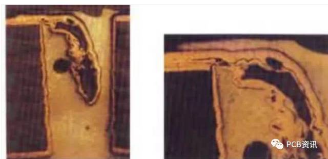
(2) Residual adhesive residue in the pattern transfer process is very important to control the process parameters, because poor pre-drying, improper temperature and pressure of the film will cause adhesive residue at the edge of the hole and cause the ring of the hole Empty. The obvious feature is that the thickness of the copper layer in the hole is normal, and a ring-shaped void appears on the single-sided or double-faced mouth, extending up to the pad, and the edge of the fault has obvious traces of etching. The graphic plating does not cover the entire board (see image 3).
(3) The amount of microetching before pre-treatment microetching should be strictly controlled, and in particular, the number of rework of dry film should be controlled. It is mainly because the plating thickness is thin due to the uniformity of plating in the middle of the hole. Excessive rework will result in thinning of the copper layer in the hole of the entire plate, and eventually produce a ring-shaped copper in the middle of the hole. The obvious feature is that the plating in the hole becomes gradually thinner, and the plating of the pattern wraps around the entire plating (see Figure 4). 3. Plating voids caused by pattern plating (1) Patterning The micro-etching of the plating micro-etching pattern must be strictly controlled, and the resulting defects are basically the same as the dry film pre-treatment micro-etching. In severe cases, the hole wall will have a large area without copper, and the thickness of the full plate layer on the surface of the board is obviously thin. Therefore, to measure the microetching rate regularly, it is best to optimize the process parameters by performing DOE experiments.
(2) Tin (Pb-Sn) poor dispersion due to poor solution properties or lack of rocking and other factors to make the thickness of the tin plating coating is insufficient, in the back of the film and alkaline etching the tin layer and copper layer in the middle of the hole erosion, Create a ring cavity. The obvious feature is that the thickness of the copper layer in the hole is normal, and the edges of the fault are clearly etched. The pattern plating does not cover the entire board (see Figure 5). In view of this situation, some tin-plating photo-agents can be added to the pickling before tin plating, which can increase the wettability of the board and at the same time increase the swing amplitude.
4. Conclusion There are many factors that cause voids in the plating layer. The most common is voids in the PTH coating. By controlling the relevant process parameters of the potions, the generation of PTH coating voids can be effectively reduced. However, other factors can not be ignored. Only through careful observation and understanding of the causes of the voids in the plating and the characteristics of defects, can we solve problems in a timely and effective manner and maintain the quality of the products. Due to my limited level of experience, I have listed some practical problems encountered in peacetime production and shared and communicated with my peers.
Slaughtering Hemp Motor Power Supply,Slaughter Power Supply,Slaughtering Hemp Motor Frequency Converter,The Slaughtering Power Supply
Jinan Xinyuhua Energy Technology Co.,Ltd , https://www.xyhenergy.com