The flyback switching power supply has a simple structure and is widely used, but its transformer leakage inductance is large, and there is a voltage spike in the switching tube. In most low-power applications, an easy-to-implement RCD clamp circuit is used to slow down the voltage spike. Here is a brief introduction. The working principle of the RCD circuit and how to determine the parameters in the clamp circuit.
The single-ended flyback switching power supply has the advantages of simple structure, electrical isolation of input and output, wide input voltage range, easy realization of multiple outputs, high reliability, low cost and the like, and is widely used in small and medium power applications. However, due to the leakage inductance of the flyback transformer, the power switch tube will cause a voltage spike when it is turned off, and must be suppressed by the clamp circuit. Therefore, the RCD clamp circuit is simple and easy to implement for low power applications. Figure 1 and Figure 2 show the voltage waveforms across the RCD clamp circuit and capacitor C in the flyback circuit.
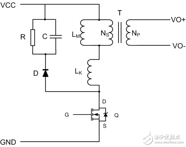
Figure 1 RCD clamp circuit in flyback 
Figure 2 Waveform at both ends of the capacitor
Suppression of leakage inductance
The leakage inductance of the transformer is not eliminated, but it can be reduced by reasonable circuit design and winding. Whether the design and winding are reasonable, the impact on the leakage inductance is obvious. With a reasonable method, the leakage inductance can be controlled to about 2% of the primary inductance.
The design should integrate the selection of the transformer core and the determination of the primary turns, so that the primary winding can be tightly wound around one or more layers of the core. When winding, the winding should be as compact and uniform as possible, so that the coil and the magnetic circuit are closer to the vertical relationship, and the coupling effect is better. The primary and secondary windings should also be as close as possible.
The excitation inductance LM is connected in parallel with the ideal transformer. The leakage inductance LK is connected in series with the excitation inductance. The leakage inductance energy in the transformer cannot be transmitted to the secondary side. If no measures are taken, the leakage inductance will release energy through the parasitic capacitance, causing voltage overshoot and oscillation, causing EMI. . To suppress its effects, the RCD clamp circuit can be connected in parallel with the transformer primary.
2. How the clamp circuit works
The RCD clamp circuit is introduced to consume the leakage inductance energy, but the main excitation inductance energy cannot be consumed, otherwise the circuit efficiency will be reduced. Therefore, the appropriate R and C values ​​should be selected during the circuit design and debugging process so that it is just consumed. Leakage energy. The following will analyze how it works.
When the switching tube Q is turned off, the voltage of the primary coil of the transformer is reversed, and the leakage inductance LK releases energy to directly charge C, the voltage of the capacitor C rises rapidly, and C discharges through R after the diode D is turned off.
If the C value is large, the voltage on C rises slowly, the secondary side has a small overshoot, and the transformer energy cannot be quickly transmitted to the secondary side. If the C value is particularly large and the voltage peak is less than the secondary side reflected voltage, the voltage on the clamp capacitor will be It is kept near the secondary side reflection voltage, that is, the clamp resistance becomes the load, and the core energy is consumed all the time. At this time, the waveform at both ends of the capacitor is as shown in Fig. 3 (a).
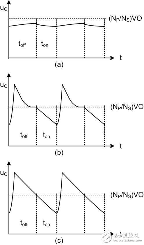
Figure 3 Waveform at both ends of the capacitor
If the RC is too small, the capacitor C will charge faster, and C will discharge quickly through the Resistor R. The leakage inductance energy consumption is very fast during the whole process. Before the Q is turned on, the clamp resistor becomes the load of the transformer, consuming the energy stored in the transformer. To reduce efficiency, the waveform at both ends of capacitor C is shown in Figure 3(b).
If the value of RC is appropriate, when the switch Q is turned on again, the voltage on the capacitor C is just placed close to the voltage reflected by the secondary side of the transformer. At this time, the clamp effect is better, and the waveform at both ends of the capacitor C is as shown in Fig. 3 (c). ) shown.
Summary
The voltage on the drain of the switch is composed of three parts: the power supply voltage, the flyback induced voltage, and the leakage inductance surge voltage. The absorption circuit must be such that it only absorbs the leakage surge voltage and does not act on the other voltage, which not only increases the burden of the absorption resistor, but also reduces the efficiency of the switching power supply.
First determine the power to be consumed by the snubber circuit:
Since the other end of the snubber capacitor is connected to the positive power supply, its voltage has only two parts: the flyback induced voltage and the leakage rush voltage. The voltage across the capacitor C is VC, the leakage inductance of the transformer is LK, and the turns ratio is n. The slope of the current leakage in the leakage inductance is:

It can be concluded that the falling time tS of the leakage current is:

Where ipk is the primary peak current of the transformer.
The voltage VC of the clamp capacitor should be determined at the lowest input voltage of the converter and at full load. Once the VC is determined, the power consumed by the snubber circuit can be calculated as:

Where fS is the switching frequency of the converter.
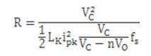
Once the power consumed by the snubber circuit is determined, the magnitude of the clamp resistor can be determined:
During the switching process of the switch, the voltage change across the clamp capacitor C is ΔVC, and the appropriate ΔVC can be taken according to the VC, thereby further determining the clamp capacitance:

Finally, the voltage VC across the clamp capacitor is determined according to the transformer reflected voltage nVO, which is usually 2 to 2.5 times. If the value is too small, it will cause large loss. The calculation of the RCD clamp circuit only determines the order of magnitude of the R and C values, and the specific parameters can be adjusted according to the actual test waveform to achieve the best results.
Power Film Capacitors - Plastic Case
Polypropylene High Voltage Capacitor,axial film capacitor,axial capacitor,SHV capacitor
XIAN STATE IMPORT & EXPORT CORP. , https://www.capacitorhv.com